


- News
5 December 2014
First 250nm-wavelength nanowire LEDs claimed
Ohio State University and University of Illinois at Chicago have developed deep ultraviolet (DUV) light-emitting diodes (LEDs) based on III-nitride semiconductor nanowires [Thomas F Kent et al, Nanotechnology, vol25, p455201, 2014]. The team says of one device emitting 250nm-wavelength radiation: “This is to our knowledge the shortest operating wavelength nanowire LED yet reported.”
DUV LEDs are being developed to avoid the use of bulky, fragile lamps based on poisonous mercury. However, the efficiencies of LEDs at wavelengths shorter than 270nm are very low. Potential applications include killing microbes and spectral analysis of biological material.
Using nanowires rather than layers of III-nitride semiconductor material allows the aluminium gallium nitride (AlGaN) material to vary over a wider range of composition without concerns arising from strain relaxation effects such as dislocation formation. Also, high-Al-content AlGaN in DUV LEDs suffers from problems in doping for hole majority carriers and in light extraction due to photon polarization effects.
Creating p-type hole injecting regions is difficult, and for DUV emission compromises have to be made. Either highly resistive p-AlGaN or photon-absorbing lower-resistance p-GaN is used. The problem with p-AlGaN is that the activation energy of the magnesium doping used is much higher than for p-GaN. On the other hand, the bandgap of GaN is smaller than the energy of DUV photons.
The Ohio/Chicago team used the polarization contrast of the chemical bonds of differing Al-content AlGaN to reduce the need for doping in the p-type region of their “polarization-induced nanowire light-emitting diodes” (PINLEDs).
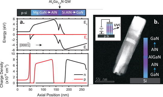
Figure 1: Polarization-induced nanowire light-emitting diodes. (a) Band diagram showing p- and n-type regions as well as the AlGaN QW active region. (b) HAADF-mode STEM micrograph showing individual heterostructure nanowire. Insert shows heterostructure schematic and device schematic.
The III-nitride nanowire heterostructures (Figure 1) were grown using RF nitrogen plasma source molecular beam epitaxy (MBE) on p-type silicon (111) substrates. The researchers avoided silicon nitride formation by rotating the substrate away from the sources during plasma lighting, tuning and the initiation of III-nitride growth.
The heterostructure began with gallium nitride (GaN) nucleated at 710°C in nitrogen-rich conditions. The devices consisted of a 100nm linearly graded GaN to AlN region, an active region of one or more quantum wells, and a 100nm linearly graded AlN to GaN region.
The growth of the p- and n-type graded regions occurred at 790°C. Also, in some devices 790°C was used for the active region, but improved performance at shorter wavelengths was found from 840°C growth.
Assuming N-polar nanowires, the researchers expected the first and second graded composition regions to give p- and n-type contacts, respectively. Although there was some magnesium doping in the p-type region, the concentration was much reduced compared to that used in commercial III-nitride DUV LEDs. The n-contact region was silicon-doped.
The researchers fabricated LEDs with pressed-on indium contacts to the silicon substrate and electron-beam evaporation of titanium/gold to a thin n-GaN layer on the upper tips of the nanowires.
Electroluminescence studies on a variety of AlGaN quantum wells grown at 790°C showed the expected monotonic blueshift of wavelength with increasing Al-content down to 290nm. However beyond 40%-Al, the wavelength became pinned at 290nm.
Photoluminescence spectral analysis showed two peaks – a peak that shifted to higher photon energy with increasing Al-content, and a broader composition independent peak around 3eV. The lower energy peak was attributed to a trap state. As the higher energy peak became pinned around 4eV, its intensity declined beyond 50% Al-content of the well. The researchers saw the quenching of the high-energy peak as being “indicative of the presence of a deep level in the active region of the device which is dominating over radiative band-to-band recombination processes”.
The researchers then produced devices with higher substrate temperature during growth of the active region with a view to avoiding oxygen incorporation that can lead to deep levels. The temperature was ramped to 840°C towards the end of the p-region growth. The quantum well region consisted of three Al0.8Ga0.2N wells with AlN barriers. The final part of the heterostructure was grown by ramping down to 790°C toward the end of the active region growth.
Contacts were made to the p-Si substrate and to a gridded pad on a 350μmx350μm region on the tips of the nanowires. Current-voltage measurements showed turn-on at 6V, corresponding to the ~6eV AlN bandgap.
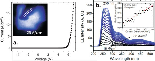
Figure 2: (a) Device I–V curve showing 6V turn-on and rectification. Inset shows image of the active device collected with an ultraviolet microscope. (b) Electroluminescence spectra of high-temperature active region device showing evolution with increasing current density. Inset shows peak power versus current density.
The new device emitted 250nm-wavelength radiation, unlike the 290nm for similar AlGaN composition devices with active regions grown at 790°C (Figure 2). However, the radiation of the new device red-shifted to 280nm as the current injection increased. This was due to a second peak at 280nm that grew as the current increased. The two peaks had equal intensity at 368A/cm2 current density. The researchers suggest that the two-peak spectral structure was due to carrier overflow/overshoot.
The output power was 2nW with 400mA injection and the external quantum efficiency (EQE) was estimated at 2μ% (2x10⁻⁶%). The researchers comment: “Although this is a very small efficiency, it is emphasized that the device geometry for such devices is far from optimized, causing a low percentage of nanowires to be contacted and requiring thick, absorbing contact layers to form coalesced tops that contact all nanowires in parallel, suggesting that significant improvements can be made with future process development.”
Optimized commercial devices at 250nm achieve efficiencies around 0.2%. Under pulsed operation to avoid self-heating, these devices achieve 0.22μW at 400mA.
The team believes that higher growth temperatures could result in shorter emission wavelengths, but that a number of challenges would need to be overcome to achieve this.
DUV LEDs Nanowires GaN AlGaN MBE
http://dx.doi.org/10.1088/0957-4484/25/45/455201
The author Mike Cooke is a freelance technology journalist who has worked in the semiconductor and advanced technology sectors since 1997.


