


- News
18 December 2014
Diamond-like carbon used to improve performance of GaN HEMTs
Researchers based in Taiwan have used micro-machining and diamond-like carbon (DLC) layers to improve the thermal performance of nitride semiconductor high-electron-mobility transistors (HEMTs) on silicon substrates [Hsien-Chin Chiu et al, Appl. Phys. Express, vol8, p011001, 2015].
HEMT performance tends to degrade when the temperature increases due to self-heating or when operated in harsh environments. Thermal management can be expensive, requiring external cooling equipment. Reducing the need for such measures requires high-thermal-conductivity materials and structures.
The team from Chang Gung University, Feng Chia University and RiteDia Inc used micro-machining to remove part of the substrate from under HEMT-based circuits, along with thermally conductive layers of DLC and titanium to improve breakdown voltages and increase maximum drain currents.
DLC has a high thermal conductivity and a similar coefficient of thermal expansion to gallium nitride (GaN). Materials with mismatched expansion coefficients can delaminate when thermally processed or when operated at varying temperatures.
The epitaxial material for the HEMT (Figure 1) was grown on p-type (111) silicon through metal-organic chemical vapor deposition (MOCVD). The 2μm buffer layer consisted of a series of layers of GaN and AlGaN. The GaN channel layer was 1μm thick. The 18nm Al0.27Ga0.73N barrier was sandwiched between the channel and a 1nm GaN cap.
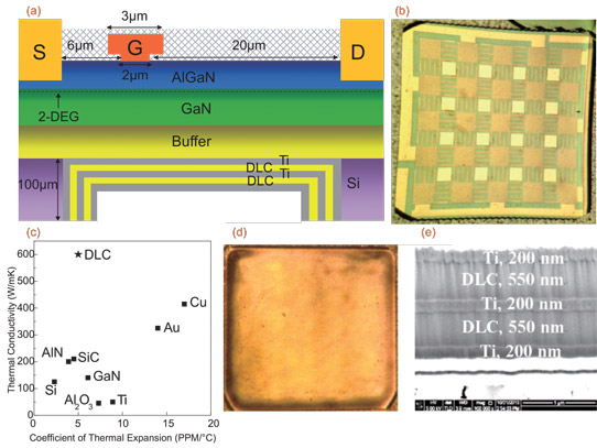
Figure 1: (a) Cross-section of AlGaN/GaN HEMT with DLC heat-dissipation layer. (b) Backside view of M-HEMT. (c) Material coefficient of thermal expansion (CTE) and thermal conductivity. (d) Backside view of M-HEMT with DLC heat-dissipation layers. (e) SEM image of DLC/Ti layers.
The HEMT structure was fabricated with a 300nm-high mesa etched from the epitaxial wafer, titanium/aluminium/nickel/gold ohmic contacts, 100nm silicon dioxide passivation, and Schottky gate. The gate was T-shaped to give a field-plate to reduce current collapse under pulsed operation. The gate had a 2μm footprint and 3μm T-head.
The layout of the devices was an air-bridged matrix (ABM) designed to improve heat distribution. The gate zigzagged between interdigitated source/drain electrodes. The active device area was 1.25mmx1.25mm. Micro-machined HEMTs (M-HEMTs) were compared with standard HEMTs without micro-machining. The gate width of the M-HEMT was 22.8mm. The standard device had a wider gate of 40mm (1.25mm/finger, 32 fingers).
After the HEMT fabrication, the substrate was thinned to 100μm from 625μm. For the micro-machining step, the silicon under the active region was removed using sulfur hexafluoride plasma etch. Further etching with boron trichloride/chlorine plasma cut partially into the transition/buffer layers.
DLC films were sputtered from a metal hydrocarbon target of tungsten carbide. Titanium layers were also applied for film adhesion and improved electrical conductivity. The DLC/titanium was applied in two pairs of thickness 200nm and 550nm, respectively, to give a total DLC thickness of more than 1μm.
The three-terminal off-state breakdown of the devices was measured in Fluorinert liquid to avoid surface flashover. The 1mA/mm breakdown of the M-HEMT with DLC/titanium film at -8V gate potential occurred with a source-drain bias of 637V. The standard HEMT broke down at 450V. Two-terminal breakdown of the buffer occurred for the M-HEMT with DLC/titanium film at 1400V and the standard HEMT at 1100V.
The M-HEMT/DLC/titanium structure also improved the transistor performance. The saturated drain current was 4.97A, compared with 2.18A for the standard device. The threshold voltage was -2.3Vfor both devices. Bending strain of 0.01% was found to reduce the maximum current 30% for the standard HEMT, but only 5% for the M-HEMT with DLC/titanium. The researchers attribute the relative insensitivity-to-bending to thermal effects and removal of silicon from under the buffer.
The increase of on-resistance with temperature up to 200°C was slower for the M-HEMT with DLC/titanium at 1.51mΩ/°C, compared with 2.77mΩ/°C for the standard HEMT. The researchers estimate the thermal resistance of the standard HEMT structure at 13.6K/W, compared with 5.3K/W for the M-HEMT with DLC/titanium layers.
Thermographs with devices with drain current at 1A with a 10V bias showed the standard HEMT to be running hotter at up to 172°C, compared with 90°C for the M-HEMT. Another M-HEMT, but without the DLC/titanium layers, had a peak temperature of 125°C.
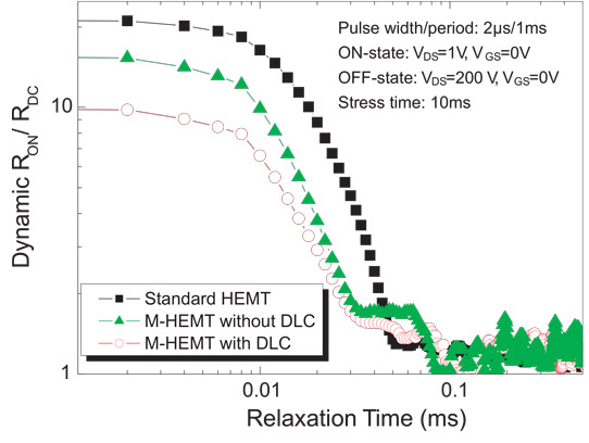
Figure 2: Dynamic switching performance of standard HEMT, M-HEMT without DLC layers, and M-HEMT with DLC layers.
The dynamic on-resistance under pulsed operation was also tested. Again, the M-HEMT with DLC/titanium layers showed improved performance (Figure 2). The poorer performance of the standard HEMTs was attributed to deep-level capture in buffer/transition layer traps and parasitic effects from the silicon substrate. Reduction of device thermal resistance is believed to be beneficial for relaxing and conducting the carriers from ON-state operation.
http://iopscience.iop.org/1882-0786/8/1/011001/article
The author Mike Cooke is a freelance technology journalist who has worked in the semiconductor and advanced technology sectors since 1997.


