


- News
31 December 2014
Gallium nitride transistors fabricated on cubic silicon carbide on silicon
Researchers in Germany have developed gallium nitride (GaN) high-electron-mobility transistors (HEMTs) on silicon carbide (SiC) layers on silicon wafers [Wael Jatal et al, IEEE Electron Device Letters, published online 11 December 2014]. The ohmic source-drain contacts were gold-free (Au-free) titanium nitride on titanium (TiN/Ti). The researchers came from Technische Universität Ilmenau and Institut für Mikroelektronik- und Mechatronik-Systeme gemeinnützige GmbH (IMMS GmbH).
GaN-based HEMTs are being developed for radio frequency (RF) power amplification, based on high operating frequencies combined with high output power. The best GaN transistors are generally produced on hexagonal (4H) poytype SiC wafers, which are expensive and are of smaller diameter than is available with silicon.
The substrate used by Jatal et al was low-resistivity (3mΩ-cm) (111)Si on which 3C cubic polytype SiC had been deposited. The SiC growth began with 3nm carbonization with ethylene (C2H4) precursor. Further SiC was grown by adding silane (SH4) as a silicon chemical vapor deposition (CVD) precursor.
Metal-organic chemical vapor deposition (MOCVD) was then used to apply 100nm aluminium nitride (AlN) as an interlayer, and GaN buffer. The barrier structure consisted of Al0.2Ga0.8N/AlN (design A) or Al0.35Ga0.65N (design B). The AlGaN barrier thickness in both cases was 20nm. The AlN spacer between the AlGaN barrier and GaN buffer of design A was 2nm. The structures were capped with 2nm GaN.
The epitaxial design A achieved a Hall mobility of 1760cm2/V-s, compared with 1200cm2/V-s for design B. The sheet carrier densities were very similar at 7.5x10¹²/cm2 for design A and 7.2x10¹²/cm2 for design B.
The nickel-gold HEMT gate had two fingers of total width 150μm. The gate was centered in the 2μm source-drain gap.
The ohmic contacts for the source-drain regions were applied using magnetron sputtering of titanium. The initial deposition was 20nm titanium followed by 100nm titanium nitride. The titanium nitride was formed through reactive magnetron sputtering in argon/nitrogen atmosphere and annealing at 850°C in nitrogen.
The specific contact resistance of Ti/TiN structures was ~10-6Ω-cm2. The contact resistance was 0.13Ω-mm. The root-mean-square (rms) roughness was 1.8nm. The researchers claim that their Ti/TiN structure is among the best gold-free structures so far.
The researchers comment: “We ascribe the low contact resistivity to the conversion of Ti into TiN causing the formation of nitrogen vacancies in the barrier layer which lead to a high doping level of the AlGaN underneath the contact.”
Table 1: Results of DC and RF characterization of 100nm-gate HEMTs. DC measurements at 10V drain-source voltage (VDS): maximum drain current (ID) and peak transconductance (gm). On resistance (Ron) measured at low drain voltage with zero gate potential. Also shown are contact resistance (RC), sheet resistance (RS), specific contact resistance ρC), and cut-off frequencies (fT) at 10V and 20V VDS (-2.75V gate potential).
| Barrier design | ID | gm | Ron | RC | RS | ρC | fT at 10V | fT at 20V |
| A | 1.13A/mm | 388mS/mm | 0.9Ω-mm | 0.13Ω-mm | 169Ω/sq | 1x10⁻⁶Ω-cm2 | 115GHz | 150GHz |
| B | 0.95A/mm | 360mS/mm | 1.6Ω-mm | 0.6Ω-mm | 365Ω/sq | 1x10⁻⁵Ω-cm2 | 79GHz | 107GHz |
The team carried out a number of characterizations on a 100nm-gate-length device (Table 1). The researchers attribute the improved performance of design A HEMTs to reduced alloy scattering due to the AlN spacer layer.
The RF measurements were carried out between 0.1GHz and 50GHz. Using extrapolations and de-embedding corrections, the cut-off frequency (fT) for an 80nm-gate HEMT at 20V drain bias and -2.75 gate potential was estimated at 176GHz. The maximum oscillation frequency (fmax) was 70GHz. The low fmax was blamed on the simple rectangular gates and low-resistance substrate that was used. “Significant improvements of fmax can be expected by using mushroom gates with reduced gate resistance and high-resistivity substrates,” the team writes.
By contrast, the best 80nm-gate Al0.35Ga0.65N/GaN HEMTs demonstrated a poor fT of only 115GHz at 20V drain voltage. HEMTs on SiC can achieve fT values of 200GHz with a 75nm gate length. The corresponding value for HEMTs on silicon is 152GHz.
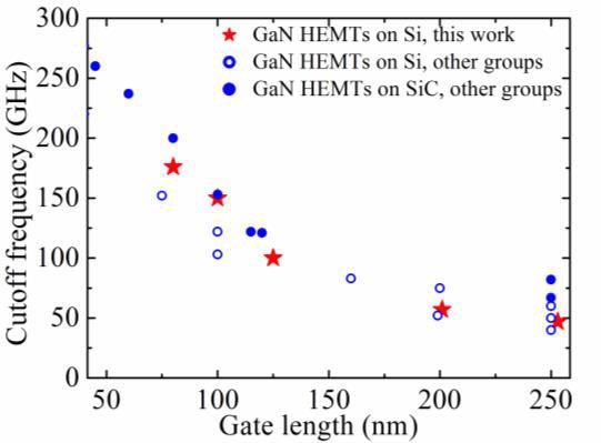
Figure 1: Comparison of cutoff frequencies of GaN HEMTs on Si with barrier design A with best data reported by other groups for GaN HEMTs on Si and on SiC.
Comparing their results with those of others (Figure 1), the researchers comment: “It can be seen that our 80nm-gate HEMT shows competitive fT performance compared to GaN HEMTs on Si (with Au-based and Au-free contacts) reported by other groups. Moreover, our GaN HEMTs on Si with barrier design A rival successfully the best reported GaN HEMTs on SiC substrates in the 80-125nm gate-length range.”
GaN HEMTs GaN AlGaN SiC Silicon wafers MOCVD
http://ieeexplore.ieee.org/xpl/articleDetails.jsp?arnumber=6982198
The author Mike Cooke is a freelance technology journalist who has worked in the semiconductor and advanced technology sectors since 1997.


