


- News
17 February 2014
Increasing fMAX for InP/GaInAsSb transistors
Researchers at ETH-Zurich have used quaternary gallium indium arsenide antimonide (GaInAsSb) in the p-type base region of a double heterostructure bipolar transistor (DHBT) to improve performance over devices using GaAsSb or graded GaAsSb/GaInAsSb [Ralf Flückiger et al, IEEE Electron Device Letters, v35, p166, 2014].
Radio-frequency measurements gave a maximum oscillation frequency (fMAX) of 636GHz and cut-off (fT) of 424GHz at a collector current density of 8.8mA/cm2 and collector emitter voltage of 1.6V. The researchers comment: “The present transistors offer the highest fMAX to date for GaInAsSb DHBTs and match the highest fMAX of any Sb-based DHBT.”
DHBTs with graded bases have achieved balanced fT/fMAX performance of 480/420GHz and unbalanced performance of 670/185GHz. ETH-Zurich has previously produced GaAsSb devices with fT/fMAX of 428/621GHz (in 2013) and 365/501GHz (in 2011).
The addition of indium to GaAsSb is expected to increase minority electron mobility, reducing base transit time and thus improving the frequency response.
The epitaxial structure (Table 1) was produced on semi-insulating indium phosphide (InP) using metal-organic vapor phase epitaxy (MOVPE). The 20nm Ga0.94In0.06As0.59Sb0.41 base layer had a sheet resistance of 1070Ω/square.
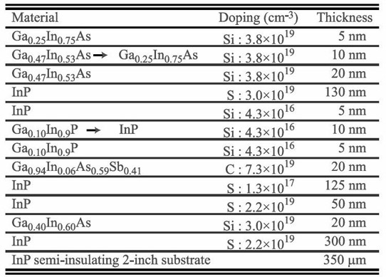
Table 1: Epitaxial layer structure for ETH-Zurich DHBT with InP collector, GaInAsSb base, and GaInP/InP emitter.
The sheet resistance value is considered relatively low considering the low doping concentration. Part of the explanation is given by the high hole mobility of 40cm2/V-s. A similarly doped GaAsSb layer with ~0.6 As fraction had a sheet resistance of 1140Ω/square and a hole mobility of 31cm2/V-s.
The DHBTs were fabricated using a triple-mesa process. The emitter area was 4.4μm x 0.3μm and the base/collector contact area was 5.0μm x 0.8μm.
With 0V bias across the base-collector junction, the peak DC gain was 23. The researchers estimate that a GaAsSb base device with similar sheet resistance would have a gain of about half of this. The open base common emitter breakdown voltage was 4.75V.
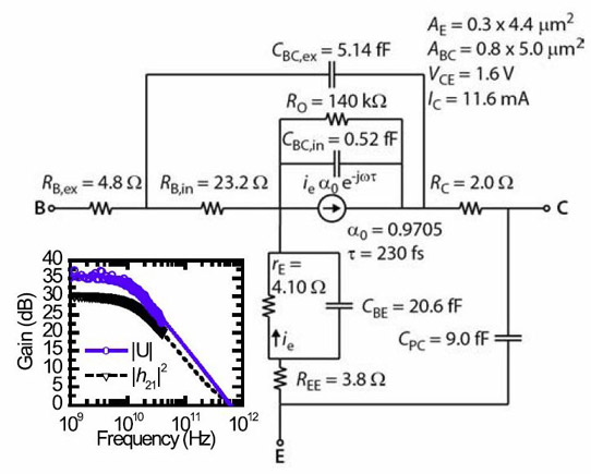
Figure 1: Small-signal equivalent circuit with component values extracted from S-parameter measurements at VCE bias of 1.6V and IC at 11.6mA. Inset: measured |h21|2 and U (symbols) with corresponding simulated small-signal data (lines).
The small-signal model for the optimum RF bias point (Figure 1) has a total base resistance of 123Ω-μm – which is 10% lower than ETH-Zurich’s 2013 GaAsSb-base DHBT.
GaInAsSb DHBTs DHBTs InP MOVPE
http://ieeexplore.ieee.org/xpl/login.jsp?tp=&arnumber=6709773
The author Mike Cooke is a freelance technology journalist who has worked in the semiconductor and advanced technology sectors since 1997.


