


- News
10 February 2014
Gallium nitride quantum dots and deep UV light emission
University of Notre Dame (UND) is developing gallium nitride (GaN) quantum dots in aluminium nitride (AlN) as a route to deep ultraviolet (UV) light-emitting diodes (LEDs) [Jai Verma et al, Appl. Phys. Lett., v104, p021105, 2014].
Aluminium gallium nitride deep-UV LEDs are being widely developed for water purification, sterilization, integrated biosensors, solid-state lighting, and lithography. “The availability of low-power, lightweight, and robust deep-UV light sources are expected to seed several unforeseeable applications,” the UND researchers add.
The leader of the research team, Debdeep Jena, also sees potential for low-threshold lasers: “Quantum-dot lasers require much lower threshold injection currents than quantum well or double-heterostructure lasers due to the reduced dimensionality. In extremely wide-bandgap semiconductors, free carriers do not come about easily because of doping problems. Thus a quantum dot active region is highly attractive for electrically injected deep-UV lasers. That is really the long-term goal driving this work.”
Presently the external quantum efficiency (EQE) of AlGaN quantum well LEDs is low (a few percent at most in the 250nm wavelength region) due to a number of challenges. A leading problem is the difficulty in injecting sufficient numbers of electrons and holes into the active region.
An additional (and related) problem is that the hole source tends to be restricted to GaN or very low Al-content AlGaN with a bandgap narrower than the emitted radiation. This means that the emitted photons are strongly absorbed by the p-contact.
The researchers see two advantages for GaN QDs over AlGaN QWs: “Three-dimensional confinement prevents electrons and holes from thermally diffusing to dislocations and recombining nonradiatively. The monolayer thickness makes the emission process robust to quantum-confined Stark effect (QCSE).”
The confinement of the electron and hole energy levels in quantum dot devices increases the bandgap, allowing higher-energy, shorter-wavelength photons to be produced. The electron injection and hole injection operate by tunneling enabled by alignment of the conduction and valence bands with the electron and hole energy levels of the confined GaN QDs, rather than the drift/diffusion of traditional devices. Tunnel injection avoids problems from self-heating effects.
To tackle the problem with the p-type hole injecting contact, the UND researchers used “polarization doping” to allow the use of wider-bandgap AlGaN rather than GaN. The technique uses changes in polarization given by grading the Al-content of the AlGaN layer to enhance the activation of the magnesium doping. Normally, high-Al-content AlGaN has a prohibitively high activation energy that kills hole densities and hence conductivity.
Growth of the semiconductor material was through plasma-enhanced molecular beam epitaxy on thick AlN-on-sapphire templates. The AlN nucleation and buffer layers were grown at 730°C. The active layers of compressively strained GaN quantum dots were formed due to the 2.4% lattice mismatch with AlN.
The photoluminescence of the GaN quantum dots can be varied by altering the growth time or Ga flux. A reduction in growth time from 35 to 25 seconds with 6.2x10⁻⁸Torr Ga flux reduces the peak wavelength from 270nm to 246nm. Also, in the longer-wavelength case, there is a secondary peak, which is much reduced in the shorter-wavelength QDs. Reducing the Ga flux to 5.6x10⁻⁸Torr with 25 second growth blue-shifts the wavelength further to 238nm.
An alternative technique with a Ga-rich flux of 2.6x10⁻⁷Torr, but interrupting the growth after 12 seconds for up to 45 seconds, gave a PL peak wavelength as short as 234nm, corresponding to a photon energy of 5.3eV. Bulk GaN has a bandgap of 3.4eV in the near UV (~365nm).
The researchers attribute the shorter wavelength from the interrupt process as being due to smaller, more confined dots as a result of Ga desorption. The QD heights were 0.58nm in 2.7nm AlN barriers, as determined in transmission electron micrograph (TEM) and x-ray diffraction analysis.
The LED active regions consisted of 8 layers of QDs. Two of the devices used the 25-second growth method, and one used the interrupted technique with 12-second growth followed by 25-second “ripening”.
The n-type electron injection region consisted of 225nm silicon-doped AlGaN. A 117nm p-type hole injection region was achieved by different techniques. One of the 25-second growth devices used a traditional uniform magnesium-doped Al0.5Ga0.5N layer (sample I). The two other samples used ‘polarization doping’ that consisted of grading the x-value of magnesium-doped AlxGa1-xN by varying the Al flux during growth. For the second 25-second growth device the grading was from 0.5 to 0.25 (sample II). The third interrupted growth device used a 0.97-0.77 grading (sample III).
The 300μm x 300μm LEDs were fabricated by etching mesas, applying titanium/aluminium/nickel/gold to the exposed n-type surface and a thin nickel/gold transparent current-spreading electrode to the p-type surface, and depositing titanium/gold p-contact pads.
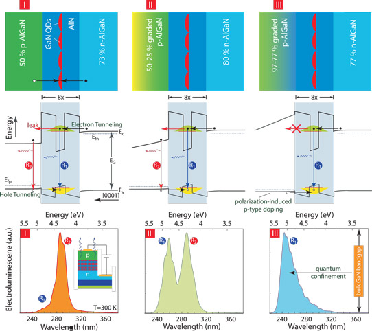
Figure 1: Schematic cross-section of GaN/AlN QD UV LEDs. Sample I: 73% n-AlGaN, 50% p-AlGaN; sample II: 80% n-AlGaN, 50%–25% p-AlGaN; sample III: 77% n-AlGaN, 97%–77% p-AlGaN. Corresponding schematic band diagrams at forward bias, showing tunneling transport and recombination mechanisms in QDs (R1) and AlGaN cladding layer (R2). Individual electroluminescence (EL) spectra for structures show short- and long-wavelength emissions.
The sample III device also blocks electron overflow (Figures 1 and 2). In fact, the sample I device has most of its emission emanating from the p-type injection region rather than the QDs. The sample II device has improved emission from the QDs, but some of this radiation is converted in the p-type region into the longer wavelength of transitions in the p-type region (down-conversion), along with emissions from electron leakage.
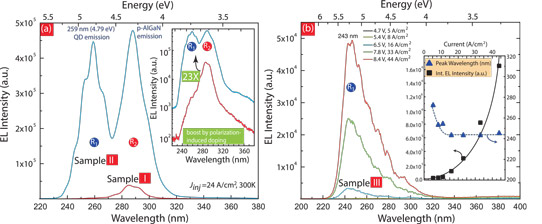
Figure 2: (a) EL spectra for graded AlGaN layer LED (sample II) showing emission from QDs (259nm) and p-AlGaN layer (290nm). Non-graded AlGaN layer LED (sample I) shows weak QD emission. EL intensity from sample II is 23 times larger than from sample I, implying better hole concentration due to polarization-induced doping. Inset: log scale EL spectra. (b) EL spectra for 97%–77% graded AlGaN layer LED (sample III) showing 243nm emission from GaN QDs grown in interrupted growth mode. Inset: EL peak wavelength and intensity variation with injection current density.
The sample III devices solve both the leakage and down-conversion problems, giving a single deep-UV peak at 243nm (5.1eV). The electron leakage is blocked by the thicker barrier to leakage and down-conversion by the wider bandgap, preventing re-absorption of QD photons.
The researchers believe further improvements could come from examining the effect of the number of periods in the active region and improving the ohmic contacts to the p-type layer, along with incorporating polarization-induced doping in the n-type AlGaN layer as well. The team is also working on fully calibrated characterization of the devices using an integrating sphere.
GaN quantum dots GaN Deep UV LEDs
http://dx.doi.org/10.1063/1.4862064
The author Mike Cooke is a freelance technology journalist who has worked in the semiconductor and advanced technology sectors since 1997.


