


- News
20 February 2014
Vertical GaN transistor with 1.6kV blocking voltage
Researchers at Japan’s Toyoda Gosei Co Ltd have achieved a blocking voltage of 1.6kV for a vertical gallium nitride (GaN) metal-oxide-semiconductor field-effect transistor (MOSFET) structure [Tohru Oka et al, Appl. Phys. Express, vol7, p021002, 2014].
“To our knowledge, the blocking voltage is the highest ever reported for vertical GaN-based transistors on free-standing GaN substrates,” the researchers write. Previous vertical GaN transistors have achieved blocking voltages up to 1kV. Vertical Schottky barrier and pn diodes have achieved blocking voltages of up to 2kV.
At the same time, the threshold voltage of +7V provides normally-off behavior, as required for automotive power semiconductor applications, which normally need thresholds greater than +3V to prevent erratic performance with false triggers due to noise etc. Such threshold voltages are difficult to achieve with lateral GaN transistor structures.
The epitaxial structure for the transistor (Figure 1) was grown using metal-organic chemical vapor deposition (MOCVD) on a commercial free-standing n+-GaN substrate with dislocation density of 3-4x10⁶/cm2.The added layers were 15μm n--GaN and 1μm p-GaN, capped with 0.2μm n+-GaN.
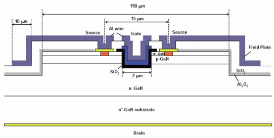
Figure 1: Schematic cross-section of trench MOSFET with field-plate edge termination.
The fabrication of the 150μm x 300μm rectangular transistors began with a chlorine-based inductively coupled plasma etch for mesa isolation, and for 2μm-wide p-body contact and 2μm-wide gate trench recessing. The gate electrode insulation was provided by atomic layer deposition (ALD) of silicon dioxide (SiO2).
The 2μm-wide p-body electrodes were palladium. The source-drain metals were titanium/aluminium, annealed at 550°C in nitrogen for 5 minutes to give ohmic contacts. The 6μm-wide source electrode was stacked on the p-body electrode to reduce the cell pitch to 15μm. The gate electrode and other wiring metals were aluminium-based.
The isolation mesa was passivated with 100nm of ALD of aluminium oxide (Al2O3). A 600nm dielectric interlayer of SiO2 was applied with plasma-enhanced chemical vapor deposition (PECVD).
A source-connected field-plate was constructed using the wiring metal to reduce electric fields at the edge of the pn junction around the isolation mesa wall by reducing potential bunching. The plate extended 10μm beyond the base of the isolation mesa.
The researchers estimate that the transistor area includes about 103 dislocations and that the active transistor area was 1.5x10⁻⁵cm2. The gate width was 2μm x 100μm.
The specific on-resistance based on the active area was 12mΩ-cm2 at 50V gate potential and 0.5V drain bias. Although this value is larger than for lateral AlGaN/GaN transistors, the researchers believe that miniaturization should result in a much smaller on-resistance while maintaining the breakdown characteristics. The gate current leakage was below the limit of the researchers’ measurement setup.
The threshold voltage of the device was +7V, indicating normally-off enhancement-mode behavior. The researchers point out that this is far short of the estimated value of +57V, based on the p-type magnesium doping concentration, gate dielectric thickness and gate electrode work-function. The team is investigating the discrepancy, which could be due to insufficient activation of the p-type doping and/or etch-related damage of the gate trench: the activation problem could be related to hydrogen incorporation; the etch process could result in nitrogen vacancies at the gate trench surface.
The off-state (0V gate) blocking voltage was measured by increasing the drain bias in steps of 5V and seeking the point at which the drain current increased by an order of magnitude between steps (Figure 2). A MOSFET without field-plate broke down at 775V. The device with field-plate edge termination achieved a 1605V breakdown.
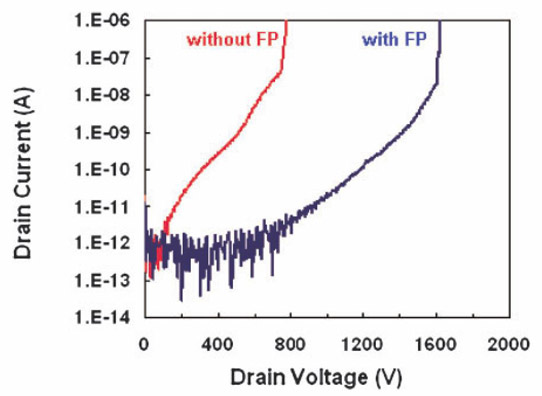
Figure 2: Off-state current-voltage characteristics for MOSFETs without and with field-plate edge termination.
The gate current in the measurements remained below the measurement limit of the researchers’ equipment. The researchers believe that the off-state leakage could be improved with optimization of the field-plate design.
GaN MOSFET GaN Free-standing GaN substrates MOCVD
http://apex.jsap.jp/link?APEX/7/021002
The author Mike Cooke is a freelance technology journalist who has worked in the semiconductor and advanced technology sectors since 1997.


