


- News
18 February 2014
Direct growth of III-V quantum dot lasers on silicon
University of California Santa Barbara (UCSB) and epiwafer foundry IQE Inc have developed 1.3μm-wavelength indium arsenide (InAs) quantum dot (QD) lasers grown on silicon (Si) with “record performance” [Alan Y. Liu et al, Appl. Phys. Lett., vol104, p041104, 2014].
The researchers write: “The device performances reported here indicates that direct growth of III-V lasers on silicon with quantum dot active regions is a competitive alternative to wafer bonding lasers grown on native substrates. Such epitaxial approaches not only provide a lower barrier to entry for silicon photonics devices through potential large-scale growth, but would also take advantage of the many benefits inherent to quantum-dot-based optoelectronics, yielding performance characteristics that are difficult to achieve in quantum well devices”.
Up to now, most demonstrations of the integration of electrically driven lasers with silicon photonic waveguides etc have used wafer bonding techniques to combine III-V and Si technologies. Silicon photonics and III-V lasers are used in optical communications. Direct growth of III-V materials is challenging and requires careful process control to achieve low defect densities.
The researchers comment that III-V quantum dot lasers “have proven to be less sensitive to non-radiative defects than their quantum well counterparts due to carrier localization within individual dots.”
The QD laser structures were grown on germanium-on-silicon (Ge-on-Si) substrates using molecular beam epitaxy (MBE). The 150mm-diameter (100) Si substrates, miscut 6° in the [111] direction, were prepared with chemical vapor deposition (CVD) of 500nm Ge.
The initial MBE included a thermal anneal to create bi-atomic step arrays for nucleation of epitaxial gallium arsenide (GaAs). This enabled the growth of mirror-like layers with reasonable dislocation densities. The GaAs growth was carried out at 600°C, giving a 1μm combined nucleation and buffer layer. The dislocation density was estimated at ~108/cm2 on the basis of transmission electron microscopic (TEM) analysis.
The substrate was then diced into smaller ‘virtual GaAs substrates’ before the laser material (Figure 1) was grown, based on two graded-index separate-confinement heterostructures (GRINSCHs) around the active quantum dot layers. The 7-period quantum dot layers consisted of InAs dots in 8nm In0.15Ga0.85As quantum wells separated by 37.5nm GaAs barriers. Some devices included p-type beryllium doping in the GaAs barriers.
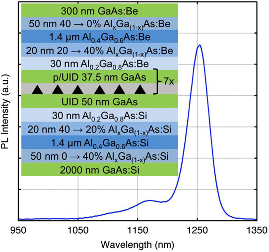
Figure 1: Room-temperature photoluminescence spectrum of the InAs quantum dots grown on Ge-on-Si substrates. Inset: layer structure of the GRINSCH InAs quantum dot lasers.
Conventional ridge-waveguide lasers were produced with gold-germanium/nickel/gold n-contacts and titanium/platinum/gold n-contacts. Plasma-enhanced chemical vapor deposition (PECVD) silicon dioxide was used for electrical isolation. The facets were polished and then the rear facet was coated with 95%-reflection material. Some devices also included silicon nitride coating on both facets, applied before the reflection material on the back facet.
At 20°C, the continuous wave (CW) threshold current and peak output power of a 937μm x 4μm device with polished facets and undoped barriers were 16mA and 50mW, respectively. The emission spectrum peaked around 1250nm wavelength, matching the peak in photoluminescence measurements.
The maximum CW lasing temperature was 110°C. Pulsed current measurements in the 20‑110°C range gave a threshold current characteristic temperature (T0) of 43K. Pulsed measurements avoid self-heating effects.
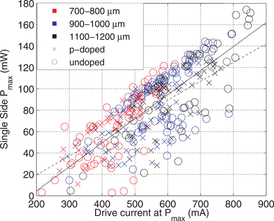
Figure 2: Maximum CW output power at 20°C (both p-doped and undoped) versus corresponding drive current. The solid and dashed lines are best fits for undoped and p-doped devices with slopes of 22.52 and 17.52 W/A, respectively.
The researchers comment: “We note that the quantum dot laser grown on Ge had nearly the same threshold as a reference laser grown on GaAs, indicating high material quality.”
An 1130μm x 10μm device with silicon nitride facet coatings and undoped barriers had a maximum power output of 176mW in CW operation, “the highest reported for telecom lasers on silicon”, according to the researchers. At 150mA, the maximum single-side wall-plug efficiency was 18% and the differential efficiency 37%.
Devices with p-doped barriers in the active region had similar characteristics. An 1155μm x 4μm with polished facets had a threshold current of 21mA and maximum output power of almost 54mW at 20°C. The T0 characteristic was 143K for the range 20-40°C and 41K for the range 40-120°C.
A second kink in the light output power versus current characteristic above the threshold kink for the device at 70°C and above was attributed to the “onset of dual-state lasing with the excited state, commonly reported for InAs quantum dot lasers where gain and carriers are not fully clamped at threshold.” In fact, the ground-state lasing is quenched above 100°C in pulsed operation and at 80°C for CW. Excited-state lasing continues up to 119°C and 130°C for CW and pulsed operation, respectively.
The researchers comment: “This is the highest CW lasing temperature for lasers on silicon, exceeding the previous record of 105°C reported for a 1.3μm AlGaInAs quantum well hybrid silicon laser.”
Averaged over 330 devices, the slope efficiencies at 20°C were 22.5W/A and 17.5W/A, for devices with undoped and p-doped barriers, respectively.
The CW output power level of 176mW and lasing temperature up to 119°C “are the highest reported for lasers on silicon,” according to the researchers.
Quantum dot lasers GaAs MBE IQE
http://dx.doi.org/10.1063/1.4863223
The author Mike Cooke is a freelance technology journalist who has worked in the semiconductor and advanced technology sectors since 1997.


