


- News
5 February 2014
Improving nanowire transistor linearity with regrowth
University of Illinois at Urbana-Champaign has realized junctionless (JL) gallium arsenide (GaAs) nanowire field-effect transistors (NWFETs) “for the first time” by implantation-free source/drain metal-organic chemical vapour deposition (MOCVD) regrowth combined with gate-all-around (GAA) metal sputtering [Yi Song et al, IEEE Electron Device Letters, published online 9 January 2014]
The researchers were particularly keen to develop devices with better linearity to minimize distortion being added between input and output signals. Radio-frequency amplification is putting greater demands on linearity than before – for example, some 4G mobile phone standards are very exacting in this respect. The usual technique to achieve this is through more complex circuitry. Apart from the increased circuit footprint, such complexity increases power demand.
The Urbana-Champaign team hopes that a better solution could come from using more linear basic transistors. “However,” the researchers point out, “non-linearity is an inherent property of conventional transistors and the transconductance (gm) non-linearity is the main contribution at high frequencies. For short-channel devices, gm linearity is especially degraded because of mobility degradation and severe source/drain (S/D) resistance. High linearity is even more difficult to achieve at low bias, which is crucial for portable RF applications.”
The researchers believe that JL GAA NWFETs are a promising route to improved linearity in scaled devices. Such devices can suffer from high parasitic S/D resistance, and the regrowth technique is a way to tackle this.
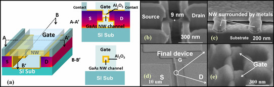
Figure 1: (a) Schematic structure of GaAs JL GAA NWFET and two cross-sectional views across (AA’) and parallel to (BB’) S/D; (b) SEM image of suspended NWs and raised S/D; (c) focused ion-beam cross section of NW surrounded by gate metal; (d) top-view SEM of fully fabricated JL GAA NWFET and (e) zoomed-in view of gate region.
The epitaxial nanowire and sacrificial aluminium gallium arsenide (AlGaAs) layers were grown on semi-insulating (SI) gallium arsenide, also using MOCVD. The layers were 100nm lattice-matched undoped Al0.6Ga0.4As and 40nm n-type Si-doped GaAs.
Source/drain regions were recessed into the epitaxial layers using wet chemical etching to avoid the surface damage cause by plasma processes. Selective MOCVD regrowth of the source/drain regions added 200nm of n-GaAs.
The nanowires were created by sculpting 140nm-high fins in the AlGaAs/GaAs epitaxial layers with dry plasma etching and then removing the sacrificial AlGaAs and silicon dioxide mask using hydrofluoric acid solution. The process resulted in 9nm x 40nm cross-section suspended nanowires of n-GaAs between the source/drain electrodes.
Further processing consisted of ammonium sulfide passivation, atomic layer deposition (ALD) of 9nm aluminium oxide gate dielectric, and 90-second 650°C annealing. The source/drain electrodes were annealed germanium/gold/nickel/gold. The chromium/gold gate metal was applied using sputtering from two directions to ensure full all-around coverage.
A device with 80nm gate length achieved a sub-threshold swing (SS) of 110 mV/dec, “reasonable for such short channels and attributed to the good GAA electrostatic control”, according to the researchers. The drain voltage was kept low (0.1-0.5V) to explore low power linearity behavior. The drain current was thus relatively low at less than 300μA/μm. Similarly, the peak transconductance was less than 400μS/μm for 0.4V drain.
The transconductance performance is relatively broad, with values near maximum for 0.2‑0.5V gate potentials. The linearity, as described by the third intercept point (IP3), was 3.8dBm for 0.4V drain and 2.6dBm for 0.3V. Even at 0.1V, IP3 is 1.5dBm, allowing use in low-bias conditions. “These values represent significant improvement over those achieved from other approaches,” the researchers comment.
The broad transconductance performance benefits power efficiency (Figure 2), as measured by the ratio of transconductance (gm) and drain current (Ids). Also the intrinsic gain of the device (transconductance/drain conductance) is greater than 4 for a large range of gate potentials.
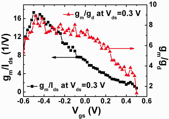
Figure 2: Power efficiency (gm/Ids, black squares) and intrinsic gain (gm/gd, red triangles) curves of a JL GaAs GAA NWFET.
The researchers attributed the improved linearity to reduced surface scattering and less mobility degradation at high bias. They add: “The reduced degradation of mobility leads to a much slower drop of transconductance when gate voltage is increased.” Another factor was reduced source/drain resistance due to the use of MOCVD regrown regions. Ion implantation of dopants is an alternative technique for reducing source/drain resistance, but it results in activation problems and crystal structure damage.
Nanowire field-effect transistors GaAs MOCVD
http://ieeexplore.ieee.org/xpl/articleDetails.jsp?arnumber=6705581
The author Mike Cooke is a freelance technology journalist who has worked in the semiconductor and advanced technology sectors since 1997.


