


- News
8 January 2014
Golden path to improved contact between graphene and gallium nitride
Researchers at Korea’s Chonbuk National University and Korea Institute of Science and Technology have improved the contact of graphene with p-type gallium nitride (p-GaN), resulting in improved near-ultraviolet (NUV) light-emitting diodes (LEDs) [Tae Hoon Seo et al, J. Appl. Phys., vol114, p223105, 2013].
It has been found that bare graphene makes a Schottky rectifying contact with p-GaN. This is due to a large difference in graphene’s work function of 4.5eV with that of p-GaN at 7.5eV. Gold bridges the gap with a work function of 5.1eV. The researchers used a thin gold (Au) interlayer between the p-GaN and graphene to convert it to an ohmic non-rectifying behavior. Further, annealing the structure caused the gold to form nanoclusters that reduced the resistance.
Gold nanoparticles have been used before to improve graphene performance as transparent current-spreading electrode. However, the new work applies the gold before the graphene rather than after (by ‘decorating’ graphene with gold nanoparticles from gold chloride solution).
The target wavelength of the LEDs was 373nm NUV (Figure 1). The metal-organic chemical vapor deposition (MOCVD) of nitride semiconductor layers on c-plane sapphire began with 25nm of low-temperature 550°C GaN, 1.5μm of high-temperature 1040°C GaN, and 2μm of high-temperature silicon-doped n-GaN.
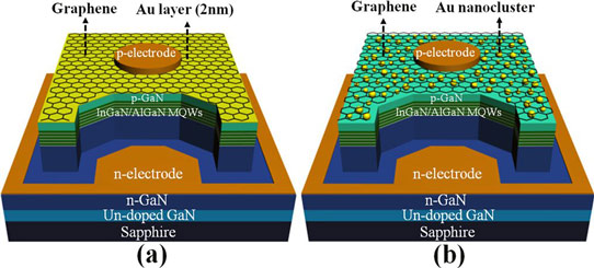
Figure 1: Schematic diagram of fabricated InGaN/AlGaN MQW-based UV LED with graphene film on (a) Au layer and (b) Au nanoclusters as transparent current-spreading electrode.
The active region consisted of a 5-period multiple quantum well (MQW) of pairs of indium gallium nitride (In0.03Ga0.97N) wells and aluminium gallium nitride (Al0.08Ga0.92N) barriers, grown at 780°C.
The high-temperature magnesium-doped p-type regions consisted of 25nm Al0.25Ga0.75N electron-blocking and 100nm GaN contact layers. The p-type doping was activated with a 940°C, 40-second anneal in nitrogen.
The 350μm x 350μm UV chips were fabricated beginning with mesa etch to expose the n-GaN contact layer, and the deposition of 2nm of gold on the p-contact. One sample was annealed in oxygen and nitrogen at 600°C for a minute, creating the gold nanoclusters.
The graphene was prepared on copper foil using chemical vapor deposition (CVD) and transferred to the LED p-contact on poly methyl methacrylate (PMMA). The samples were then annealed again at 500°C for 30 minutes in hydrogen and argon, preventing oxidation and removing the PMMA film. The graphene film was then patterned and etched in oxygen plasma.
The fabrication process was completed with the deposition of chromium/gold electrodes on the n-GaN and graphene p-contact.
Independent measurements on silicon dioxide/silicon substrates suggest that the gold clusters have a diameter of order 30nm with a density of 1010/cm2. Transmittance tests at 373nm on glass give 92.8% for bare graphene, 78% for graphene on gold, 82.7% for graphene on gold nanoclusters, and 60% for indium tin oxide (ITO). Respective electrical sheet resistances were 500±60Ω/square, 200±20Ω/square, 150±20Ω/square and 48±2Ω/square.
It is believed that the high resistance of bare graphene is due to defects inherited from the crystal grains of the copper foil growth substrate. The researchers comment that the gold layer or nanoparticles can bridge the high-resistance regions around the defects. The lower resistance of the nanoclusters is attributed to the Au nanoparticle and graphene composite providing a doping effect from direct charge transfer between the components.
Current-voltage measurements using the circular transfer length method showed that the gold interlayer converted the Schottky contact of bare graphene on p-GaN to an ohmic contact. Annealing to form nanoclusters reduced the specific contact resistance to 18mΩ-cm2, from 800mΩ-cm2 without annealing.
The reduction in specific contact resistance by thermal annealing is attributed to “the combined effects of the reduced Schottky barrier height caused by the shift of the surface Fermi level toward the valence-band edge, increased carrier concentration owing to the generation of gallium vacancies upon thermal annealing, and enhanced tunneling transport caused by a strong enhancement in the electric field through interfacial nanostructures.”
The graphene with gold nanoclusters showed the brightest electroluminescence (EL) at 20mA injection (Figure 2). The EL response of the bare graphene was the poorest and the forward voltage of the bare graphene LED was also very high at 7.2V. High forward voltage indicates energy losses through resistive effects.
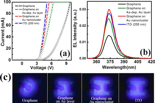
Figure 2: (a) Current-voltage characteristics, (b) electroluminescence spectra and (c) photography at 20mA injection current in InGaN/AlGaN MQW NUV-LEDs with various transparent current-spreading electrodes.
By inserting the gold interlayer and annealing to form nanoclusters, the forward voltage was reduced progressively to 4.25V and then 4.02V. The comparison sample with a conventional 200nm ITO transparent conducting electrode had a forward voltage of 3.94V at 20mA, but at slightly reduced electroluminescence compared with the gold-nanocluster graphene, which was about 10% brighter.
In addition to poor performance at 20mA, the bare graphene LED suffered from burn-out at higher currents. The photographs in figure 2c show that bare graphene also has poor current-spreading capability, with most of the illumination concentrated around the p-electrode.
The researchers comment further: “When using the graphene on Au layer and Au nanocluster, a bright and uniform light emitting was observed in the whole emission area due to effective current spreading by reduced sheet resistance. Also, the UV LED with graphene on Au nanoclusters does not show any joule heating or oxidation up to the injection currents of 100mA investigated in this work and operates without any degradation under continuous current injection up to 300s.”
Near-ultraviolet LEDs Graphene GaN MOCVD
http://dx.doi.org/10.1063/1.4836835
The author Mike Cooke is a freelance technology journalist who has worked in the semiconductor and advanced technology sectors since 1997.


