


- News
28 January 2014
PLD/MBE m-plane gallium nitride on lithium gallate
South China University of Technology has improved the quality of non-polar m-plane nitride semiconductor layers on lithium gallate (LiGaO2) by combining pulsed laser (PLD) and molecular beam epitaxy (MBE) deposition techniques [Weijia Yang et al, J. Mater. Chem. C, vol2, p801, 2014].
Non-polar nitride semiconductors are of interest for producing higher internal quantum efficiency (IQE) and hence more efficient light-emitting devices. However, the growth of non-polar material is difficult to achieve with sufficient quality or at low cost.
LiGaO2 (100) is an attractive substrate for m-plane gallium nitride (GaN) deposition because it has a lattice mismatch as small as 0.1%. Also, the thermal expansion coefficient is more nearly matching, compared with alternatives. Thermal expansion mismatch creates problems in processes involving temperatures up to 1000°C.
One drawback with LiGaO2 is that the lithium component tends to evaporate at raised temperature, as needed for MBE or metal-organic chemical vapor deposition (MOCVD).
PLD has been used to grow m-plane GaN at relatively low temperature, avoiding lithium evaporation, but the quality of the resulting material has not been sufficient for applications such as light-emitting diodes (LEDs) or laser diodes (LDs).
The researchers have designed a tool that allowed both PLD and MBE to be carried out in one ultrahigh-vacuum chamber. The system had access to gallium and indium MBE sources, along with a liquid gallium PLD target. The laser source was an external 248nm-wavelength krypton fluoride excimer laser focused through optical lenses on the target.
The LiGaO2 wafer was first annealed at 1000°C for 4 hours and cleaned to give an atomically flat surface free of contamination. After putting the wafer in the vacuum chamber and pumped down to 5x10-11Torr, the laser was used to ablate Ga with 220mJ pulses at 20Hz frequency. The substrate was positioned 5cm away and heated to 200°C. For the nitrogen source, N2 gas was pumped in at 6x10⁻³Torr pressure and put through a purifier and a 500W radio-frequency plasma radical generator.
The PLD was used to grown 50nm of m-plane GaN as a template for further GaN layers: 300nm through 500°C MBE, and 2μm through 750°C MBE.
The GaN(1100) x-ray rocking curves show improved crystallinity in the upper layers, as indicated by narrower full-width at half maximum (FWHM) values: 0.55° for the PLD layer, 0.14° for the 500°C MBE, and 0.098° for the final 2μm layer. These values compare very favorably with the 0.25° previously achieved in a PLD-only approach.
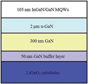 Figure 1: Schematic structure of InGaN/GaN MQWs grown on LiGaO2(100) substrates.
The PLD/MBE layers are estimated to have dislocation densities of 1.6x10¹⁰/cm2, 1.1x10⁹/cm2, and 5.1x10⁸/cm2, respectively.
The researchers checked that no lithium diffused from the substrate into the overlying GaN layer with x-ray photo-electron spectroscopy (XPS) that showed the initial low-temperature m-plane GaN buffer had suppressed Li diffusion from the substrate.
To demonstrate the possibilities for LED production, the researchers added a 7-period InGaN/GaN (3nm/12nm) multiple quantum well (MQW) structure with 700°C MBE (Figure 1). The indium composition of the wells was 0.156. The InGaN layers were estimated to have a dislocation density of 6.6x10⁸/cm2, on the basis of an x-ray rocking curve FWHM of 0.11°.
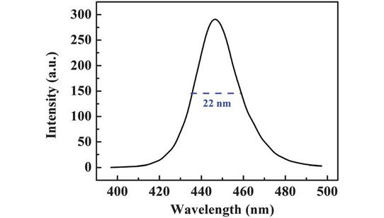
Figure 2: Room-temperature photoluminescence spectrum of non-polar m-plane InGaN/GaN MQWs on LiGaO2 substrate.
Photoluminescence measurements gave a peak at 445nm and a FWHM of 22nm (Figure 2), “comparable to the commercially available LEDs and semi-polar InGaN/GaN LEDs”, according to the researchers.
LEDs Semi-polar LEDs LDs InGaN GaN MQW MBE
http://dx.doi.org/10.1039/C3TC31935K
The author Mike Cooke is a freelance technology journalist who has worked in the semiconductor and advanced technology sectors since 1997.


