


- News
8 July 2014
BluGlass demos 10-fold improvement in RPCVD p-GaN light output
BluGlass Ltd of Silverwater, Australia has demonstrated what it says is the best ever p-GaN light output using its propriety remote-plasma chemical vapor deposition (RPCVD) technology on an metal-organic chemical vapour deposition (MOCVD) partial LED structure. This is a more than 10-fold improvement in LED efficiency over the first p-GaN demonstration data that it reported in December 2012, when the same measuring methodology is applied.
This has been achieved by making improvements in addressing the ‘interface challenge’, a key technical hurdle that has been limiting the p-GaN performance demonstration in the past.
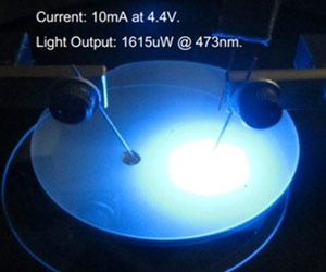 Picture: Light emission at 473nm (with full width half maximum of 22nm) from RPCVD p-GaN layer grown on MOCVD partial structure.
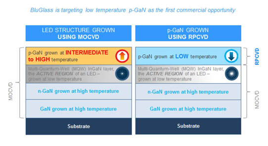
Spun off from the III-nitride department of Macquarie University of Sydney, Australia in 2005, BluGlass developed a low-temperature process using RPCVD to grow materials including gallium nitride (GaN) and indium gallium nitride (InGaN) on glass substrates, potentially offering cost, throughput and efficiency advantages for the production of LEDs and concentrated solar cells.
BluGlass says that the recent breakthroughs are the result of the enhanced plasma system in combination with new process steps that are now yielding continual performance improvements as the firm furthers progress towards its ‘Brighter LEDs’ milestone.
“The RPCVD p-GaN based LED performance in the last month has undergone a step change improvement,” notes chief technology officer Dr Ian Mann. “This has been achieved by focusing on two key aspects – the process steps for initiating the RPCVD p-GaN growth; and in finalizing the last layers grown by MOCVD – in effect, making sure the RPCVD and MOCVD steps are compatible,” he adds. “Following these recent developments, we are confident that the team is on the right path to demonstrate that low-temperature RPCVD can enhance the performance of LEDs fabricated solely by MOCVD today.” BluGlass aims to demonstrate that an RPCVD top layer (the p-GaN layers) can improve the light output of an LED.
Additionally, the firm’s BLG-300 next-generation RPCVD system is nearing completion and is expected to be growing GaN later in July. This ex-production-scale system is significantly larger than the current R&D workhorse and will effectively double BluGlass’ R&D capacity. The firm says that having multiple RPCVD systems will greatly enhance the team’s capability to address the LED milestones, the scaling of the technology towards 8” wafer deposition, and the potential performance advantages of a low-temperature CVD process for GaN-on-silicon.
BluGlass commissions former production MOCVD system to grow MQW base structures
BluGlass’ low-temperature RPCVD-grown p-type GaN films match MOCVD-grown electrical properties
BluGlass reports preliminary results on RPCVD-grown p-GaN


