


- News
14 July 2014
Band engineering for improved photo-electro-chemical etch
Researchers from Ohio State University (OSU) and University of California–Irvine (UCI) have developed a band engineering technique to improve the results from photo-electro-chemical (PEC) etch of nitride semiconductors [Prashanth Ramesh et al, Appl. Phys. Lett., vol104, p243503, 2014]. Although the etch process was used to create micro-cantilever structures, the researchers also see potential for optoelectronic applications.
PEC etch uses the narrower bandgap of indium gallium nitride (InGaN), compared with gallium nitride (GaN), to selectively remove material. The technique uses excitation of electrons and holes in the sacrificial layers, and an electrochemical bias, to enhance the etching of InGaN.
The OSU/UCI researchers tested the inclusion of 10nm highly n-type layers that simulations suggested would reduce the band-bending effect at the top and bottom of a 200nm sacrificial layer of 5% InGaN. These band-bending effects concentrate the PEC etch in the middle of the sacrificial layer. The band bending also raises a barrier to the extraction of electrons through the substrate electrode. Both factors lead to incomplete etching of the sacrificial layer.
The highly doped ‘guard’ layers provide charge that compensates for polarization charges that are induced at the interfaces between the GaN and InGaN layers. The researchers comment: “This results in a flat energy band in the entire InGaN layer, allowing uniform distribution of holes, with the energy bands aligning with those in the undoped GaN region”.
The guard layers also prevent holes from drifting out of the InGaN and allow efficient extraction of electrons through the InGaN/GaN template interface.
The materials for the OSU/UCI PEC etch (Figure 1) were produced on GaN/sapphire templates from Kyma Inc using a Veeco Gen930 molecular beam epitaxy (MBE) system. The deposition process was nitrogen plasma assisted.
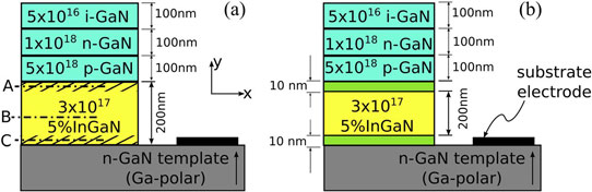
Figure 1: (a) Control stack and (b) test stack structures. Unlabeled 10nm layers in (b) are highly n-type (4x10¹⁹/cm3) GaN.
The materials were patterned with a titanium/nickel etch mask to create a large array of micro-cantilever structures of width 5−40μm and length 100−400μm. The mask allowed mesa structures to be formed using a chlorine-based reactive ion etch down to the template layer. The mask was removed to allow better penetration of radiation from a xenon ultraviolet lamp. The radiation from the lamp was filtered by another GaN/sapphire template wafer from Saint Gobain Crystals so that the radiation energy was below that of GaN’s bandgap. The substrate electrode for the electro-chemical part of the etch process consisted of titanium/gold. The counter electrode was platinum. A 1 molar (1mole/liter) solution of potassium hydroxide was used as electrolyte. The PEC etch was carried out for 30 minutes with a +1V bias between the substrate and counter electrodes.
A ‘control’ stack without the highly doped ‘guard’ layers resulted in distorted micro-cantilevers with a radius of curvature of 40μm. The curving of the cantilevers is attributed to residual stress gradients from unetched InGaN sacrificial material. The control cantilevers also suffered from cracking and warping of the anchor regions.
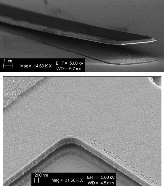
Figure 2: Scanning electron microscope (SEM) images of micro-cantilevers etched using test stack.
The ‘test’ stack with ‘guard’ layers, by contrast, gave cantilevers with “relatively minor residual curvatures and no cracking or warping of the anchor areas” (Figure 2). The researchers comment: “The minor residual curvatures seen with the use of the test stack are comparable to those reported elsewhere and are attributed to linear stress gradients due to sapphire and the metallization. These results also strongly suggest that the sacrificial InGaN layer was almost completely removed, proving the effectiveness of the proposed guard layers.”
Photo-electro-chemical etch InGaN Kyma Veeco MBE
http://dx.doi.org/10.1063/1.4883890
The author Mike Cooke is a freelance technology journalist who has worked in the semiconductor and advanced technology sectors since 1997.


