


- News
22 July 2014
Working toward lasers for on-chip global interconnects
Tokyo Institute of Technology has claimed the first room-temperature continuous-wave (RT-CW) operation of a lateral-current-injection (LCI) gallium indium arsenide phosphide (GaInAsP) membrane Fabry-Perot (FP) laser bonded to a silicon substrate [Daisuke Inoue et al, Appl. Phys. Express, vol7, p072701, 2014].
The researchers believe their work could lead to ultralow-power-consumption lasers for on-chip optical interconnections. The aim would be to use such a laser in conjunction with on-chip waveguides to replace copper global interconnects that suffer from signal delays and Joule heating effects.
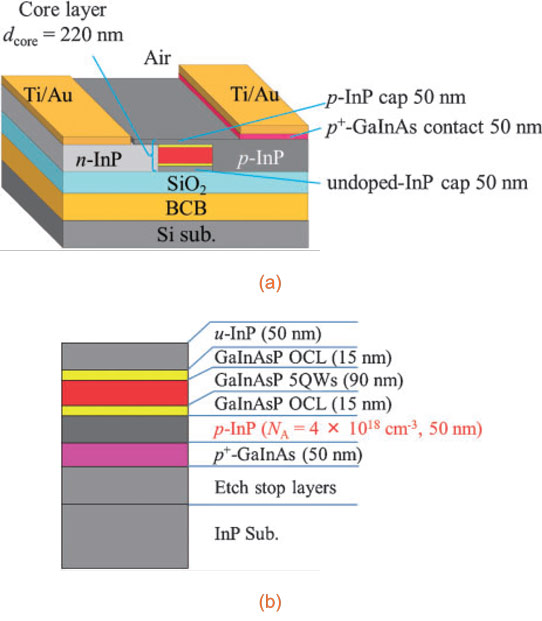
Figure 1: (a) Schematic structure of membrane laser on Si substrate and (b) initial heterostructure.
The semiconductor heterostructure for the laser (Figure 1) was grown on n-type indium phosphide (InP) substrate using molecular beam epitaxy (MBE). The five quantum wells (QWs) in the active region consisted of 1% compressively strained 6nm Ga0.22In0.78As0.81P0.19 in 0.15% tensile-strained 10nm Ga0.26In0.74As0.49P0.51 barriers. The 15nm optical confinement layers (OCLs) were also of GaInAsP.
Before the laser was transferred to the silicon substrate, the lateral-current-injection structures were created using reactive ion etching and a two-step organometallic vapor phase epitaxy (OMPVE) of the n-InP and p-InP contact regions on either side of the 0.7μm-wide device mesa stripe.
The top of the structure was covered in 1μm of silicon dioxide. The host silicon substrate was prepared with a 2μm layer of spin-coated benzocyclobutene (BCB) adhesive, pre-cured at 210°C in nitrogen. The laser wafer was flipped onto the host silicon and bonded at 25kPa pressure at 130°C, followed by hard-curing at 250°C for an hour in nitrogen.
Selective etching was used to removed the InP substrate and etch stop layer. The p+-GaInAs was also removed except for the p-electrode region. The p-InP cap layer was etched away from the n-electrode region. Finally, the titanium/gold (Ti/Au) electrodes were applied.
The structure was cleaved into Fabry-Perot lasers of various cavity lengths. A 350μm-long device had a threshold current of 2.5mA (1100A/cm2 density) in room-temperature continuous-wave operation. The external differential quantum efficiency was 22% from each facet (44% in total). The output power was 1.1mW at 10mA.
By analyzing the performance of lasers with different cavity lengths, the researchers estimate an internal quantum efficiency (IQE) of 75% and a waveguide loss of 42/cm. The internal quantum efficiency is close other vertical lasers and LCI membrane lasers on semi-insulating InP produced previously by the researchers. The team comments: “This indicates that non-radiative carrier recombination at both the top and bottom surfaces of the membrane structure are almost negligible, which is attributed to 50nm-thick InP cap layers as well as high-quality buried heterostructure interfaces prepared by two-step OMVPE re-growth. In addition, this high internal quantum efficiency indicates that there is minimal leakage current through the p-InP cap layer to the n-InP layer.”
The waveguide loss, however, is significantly higher than the 5.1/cm achieved for LCI lasers on semi-insulating InP at Tokyo Institute of Technology. The researchers suggest that scattering losses may have arisen from the side-wall roughness of the re-growth interface between the mesa stripe and the InP cladding layers.
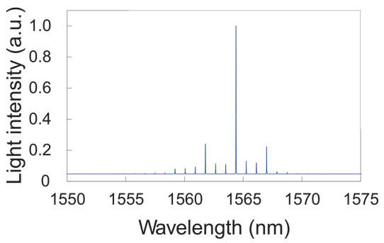
Figure 2: Spectrum of LCI membrane FP laser with 370μm cavity length and 0.7μm stripe width. Bias at twice threshold current of 2.5mA.
The emission wavelength was around 1565nm (Figure 2).
LCI GaInAsP membrane FP laser GaInAsP MBE
http://iopscience.iop.org/1882-0786/7/7/072701/
The author Mike Cooke is a freelance technology journalist who has worked in the semiconductor and advanced technology sectors since 1997.


