


- News
9 June 2014
Optimizing ammonia-based MBE for gallium nitride electron mobility
University of California Santa Barbara (UCSB) and National Taiwan University (NTU) have been optimizing ammonia-based molecular beam epitaxy (MBE) for gallium nitride (GaN) growth on a range of substrates [Erin C. H. Kyle et al, J. Appl. Phys., vol115, p193702, 2014].
The researchers claim their highest single-die electron mobility of 1265cm2/Vs at 296K (‘room temperature’, RT) for films grown on low-threading-dislocation-density (TDD) free-standing (FS) GaN templates as “the highest RT bulk GaN electron mobility to date”. To back up the claim, the paper quotes a number of results from other groups (Table 1).
Table 1: Room-temperature mobility of GaN grown by a variety of methods by different groups.
| Method | Mobility (cm2/V-s) | Year |
| HVPE | 1245 | 2001 |
| MOCVD | 1005 | 2006 |
| Ammonothermal | 265 | 2007 |
| N-rich PAMBE | 1150 | 2007 |
| Ga-rich PAMBE | 1191 | 2000 |
| NH3-MBE | 560 | 1999 |
| UCSB/NTU | 1265 | 2014 |
The researchers used a Veeco Gen 930 molecular beam epitaxy system with an unheated showerhead injector for the delivery of purified ammonia (NH3). The gallium, silicon and magnesium came from standard effusion cells.
The templates were isolated from the active region of the bulk GaN by a structure consisting of an intrinsic layer sandwiched between lightly and heavily Mg-doped p-type GaN regions (Figure 1). The isolation ensured that negligible current flowed through the template or re-growth interface. Heavily Mg-doped GaN tends to result in rough surfaces. The undoped and lightly doped top layers of the isolation gave a smooth surface for further growth.
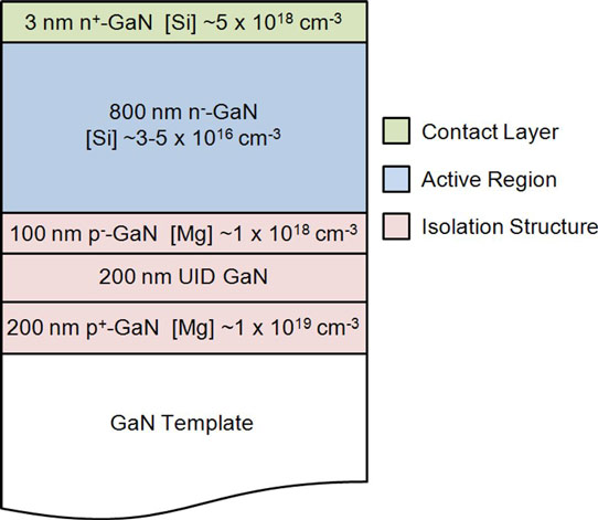
Figure 1: Schematic of UCSB/NTU growth structure.
The bulk of the structure consisted of lightly Si-doped n-type GaN with a final layer of heavily doped material “to facilitate the formation of high-quality low-resistance ohmic contacts”.
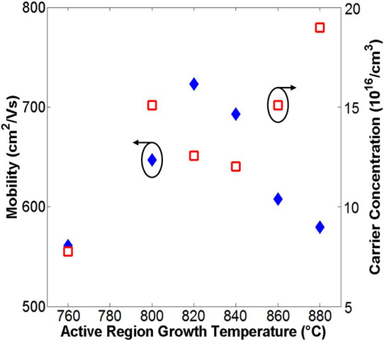
Figure 2: Average bulk electron mobility (solid blue diamonds) and average carrier concentration (red open squares) as function of active region growth temperature.
The growth was optimized with respect to temperature (760-880°C) and Si-doping concentration (~3x10¹⁶ − ~2x10²⁰/cm3). Lumilog provided the semi-insulating iron-doped GaN:Fe on sapphire templates. The ammonia flow rate during optimization was 200 standard cubic centimeters (SCCM), giving a growth rate of 7.4nm/minute. The highest mobility of more than 700cm2/V-s occurred in 820°C growth (Figure 2). The optimum silicon doping was found to be ~3x10¹⁶/cm3 (Figure 3). Mobility decreases with increased doping, while some doping is needed to make an ohmic contact with metal electrodes.
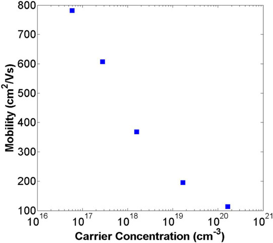
Figure 3: Effect of carrier concentration on electron mobility for GaN grown with optimized growth conditions.
Further experiments (Table 2) involved growth on a variety of templates where the ammonia flow rate was 200 or 1000 (SCCM) with the aim of quantifying the effects of TDDs. Naturally, the highest-mobility results came from using free-standing GaN templates with low TDDs. The researchers carried out a wide range of experimental and theoretical analyses to explore the impact of TDDs on the electrical performance of the GaN film.
Table 2: Single-die Hall measurements for 200SCCM and 100SCCM ammonia flow TDD series. Full-width at half maximum (FWHM) is for ω-scan x-ray diffraction from GaN (20-21) planes.
TDD-200 Series
| TDD (/cm2) | RT mobility (cm2/Vs) | RT carrier concentration (/cm3) | Highest mobility (cm2/Vs) | Highest mobility temp. (K) | FWHM (arcsec) |
| ~3x10⁷ | 1256 | 4.48x10¹⁶ | 2948 | 116 | 225 |
| ~5x10⁸ | 961 | 3.50x10¹⁶ | 2396 | 115 | 382 |
| ~5x10⁹ | 204 | 4.9x10¹⁶ | 343 | 154 | 739 |
TDD-1000 Series
| TDD (/cm2) | RT mobility (cm2/Vs) | RT carrier concentration (/cm3) | Highest mobility (cm2/Vs) | Highest mobility temp. (K) | FWHM (arcsec) |
| ~2x10⁶ | 1265 | 3.73x10¹⁶ | 3327 | 113 | 90 |
| ~5x10⁸ | 966 | 2.09x10¹⁶ | 2637 | 112 | 375 |
| ~2x10¹⁰ | 317 | 1.33x10¹⁷ | 348 | 212 | 1370 |
http://dx.doi.org/10.1063/1.4874735
The author Mike Cooke is a freelance technology journalist who has worked in the semiconductor and advanced technology sectors since 1997.


