


- News
14 March 2014
Bipolar diffusion injection into indium gallium nitride quantum wells
Aalto University in Finland has developed a new current injection method for nitride semiconductor light-emitting diodes based on bipolar diffusion [L. Riuttanen et al, Appl. Phys. Lett., vol104, p081102, 2014]. The active light-emitting multiple quantum well (MQW) region of the new device is placed under both the p- and n-type contact layers (Figure 1). This is in contrast to the usual arrangement of conventional LEDs where the indium gallium nitride (InGaN) MQWs are sandwiched between the n- and p-contacts.
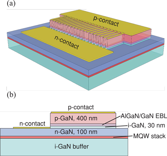
Figure 1: (a) Schematic of device and (b) layer structure and thicknesses. InGaN/GaN MQW stack is located under both p- and n-layers away from pn-junction.
The researchers believe that such work could lead to devices that could challenge conventional structures for selected applications. “In particular, it would enable a new way to inject current to nanowires and near surface structures as well as fabrication of large-area devices with improved current spreading.”
Based on previous simulations and other preparatory design work, the team has now realized these diffusion-injected LEDs (DILEDs) experimentally. The DILED was grown by metal-organic chemical vapor epitaxy (MOVPE) on a 3μm unintentionally doped GaN buffer on c-plane sapphire. The MQW consisted of 5 InGaN wells in GaN barriers.
The n- and p-type contact layers were patterned and etched down to the n-type contact layer to create a p-type mesa with a comb structure with 20μm x 300μm-long, 30μm-wide fingers/teeth. The n-type contact metals were titanium/gold. The pad extended in between the fingers/teeth of the p-type comb. The p-contact metals were nickel/gold/titanium/gold.
At low injection of 20mA, most of the electroluminescence (Figure 2) is in a broad yellow band. At high injection, e.g. 160mA, the yellow band disappears, leaving the 450nm wavelength of the MQW. The measured output power was for light emitted through the back-side of the device.
The yellow band emission could be due to “shallow dopants in n-GaN, carbon impurities in i-GaN or gallium vacancy complexes in i-GaN”. Microscopic inspection indicated that the yellow emission came from the mesa.
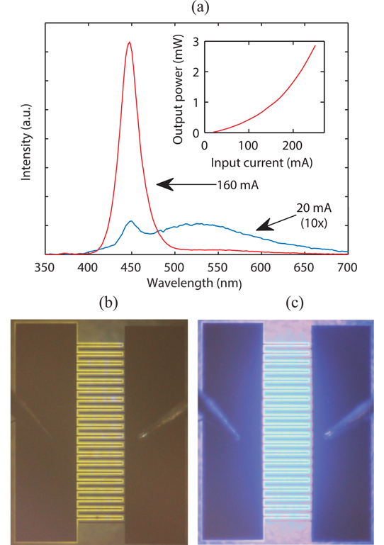
Figure 2: (a) Electroluminescence spectra of DILED at injection currents of 20mA and 160mA at room temperature. Intensity of 20mA graph is scaled by factor of 10 to show spectrum line-shape. Inset: optical power for 400-500nm emissions versus input current. (b) Low and (c) high injection current DILED micrographs.
The blue emission was found to originate mostly from the finger/teeth regions. “Since the QWs are located far outside the pn-junction, this indicates that both electrons and holes are transported to the QWs from the same side of the active region through bipolar diffusion,” the researchers write.
There was no blue-shift, which is normally observed in conventional MQW LEDs at increasing current. The researchers comment: “This suggests that the electric field inside the QWs is much less dependent on the external bias voltage than in conventional III-N LEDs.”
The bias voltage at 20mA was 3.9V and at 160mA was 5.8V. “The relatively high bias voltages are expected to be mainly caused by the unoptimized metal contacts as well as the resistance of the thin n-GaN layer of the DILED structure,” the researchers explain. They add that the current-voltage characteristics of the device were comparable with those of conventional InGaN/GaN MQW LEDs.
Using the area of the p-type mesa as the effective area of the device, an injection current of 250mA corresponds to 40A/cm2. The output power increases superlinearly, unlike conventional devices that begin to show efficiency droop effects at these injection levels. This is probably due to the low carrier densities in the MQW “caused by low injection efficiency of the unoptimized device structure”.
The external quantum efficiency (EQE) was low at around 0.4% at 250mA injection. The EQE curve increases at high current. The researchers suggest that the usual degradation of internal quantum efficiency at the higher temperatures or higher current is counterbalanced by improved diffusion of carriers into the MQW active region. The back-side temperature at 250mA current was 70°C, due to Joule heating and non-radiative recombination effects. The estimated junction temperature was 80°C. A cooling flow of room-temperature nitrogen reduced the optical output power.
The researchers performed simulations on a simplified structure with a single quantum well of 10nm and 20nm p-AlGaN electron-blocking layer. They report: “The hole concentration decreases as a function of depth as the holes diffuse deeper into the n-GaN. Despite the low hole concentration at the edge of the n-GaN region next to MQW stack, the MQW stack acts as a drain and both electron and hole concentrations increase drastically in the active region. Additionally, just above the active region the electron concentration decreases because the active region efficiently captures electrons from the n-GaN layer.”
A thick depletion region forms below the MQW active region with reduced electron and hole concentrations.
The low ~0.4% EQE measurement was reflected in a simulated injection efficiency of ~4%, the order of magnitude difference being attributed to light extraction efficiency problems. The researchers believe the injection can be improved with optimization of “layer thicknesses and doping levels as well as reducing finger widths closer to the diffusion lengths of the carriers”.
LEDs InGaN GaN MQWs InGaN MQWs MOVPE
http://dx.doi.org/10.1063/1.4866343
The author Mike Cooke is a freelance technology journalist who has worked in the semiconductor and advanced technology sectors since 1997.


