


- News
7 March 2014
Selective III-V re-growth multi-gate transistor boosts performance
Lund University has developed multi-gate (MuG) III-V metal-oxide-semiconductor field-effect transistors (MOSFETs) with a cut-off frequency of 210GHz and a maximum oscillation frequency of 250GHz, “the highest of any reported III–V multiple-gate MOSFET” [Cezar B. Zota et al, IEEE Electron Device Letters, published online 12 February 2014]. The researchers see potential post-10nm complementary metal-oxide-semiconductor (CMOS) logic and high-frequency applications.
The high performance was achieved by creating fins through selective area re-growth processes that avoided etching of the III-V material. Etch processes, particular those which are plasma-based, cause surface damage that reduces carrier mobility and hence impairs performance.
Thin stripes of hydrogen silesquioxane (HSQ) on iron-doped (100) indium phosphide (InP) substrates were patterned using electron-beam lithography (Figure 1a). The stripes were aligned with the [001] crystal direction. The HSQ material was cured at 350°C.
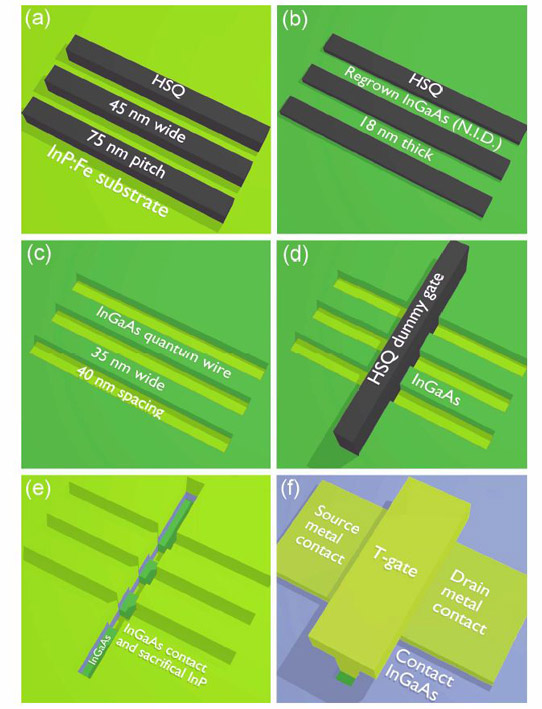
Figure1: Schematic of process flow. In fabricated devices, fins were at 45° relative to gate.
Metal-organic vapor phase epitaxy (MOVPE) was used to create channels on the InP of 3nm InP followed by 15.5nm of indium gallium arsenide (In0.53Ga0.47As) (Figure 1b). The growth temperature was 500°C. The III/V precursor ratio was 94. The fins expanded by about 5nm in width compared with the spacing between the HSQ stripes due to mask overgrowth (Figure 1c). The HSQ was removed with a (wet) buffered oxide etch.
A second re-growth step was prepared with the placement of an HSQ strip across the fins as a [110] dummy gate aligned 45° with respect to the fins (Figure 1d). The 45° angle was chosen to give the optimal facets for crystal re-growth, minimizing mask overgrowth. The deposition of 25nm In0.53Ga0.47As and 15nm In0.63Ga0.37As contact layers was followed by 90nm InP as a sacrificial support layer (Figure 1e).
The HSQ was removed and the samples were treated by immersing in 10% diammonium sulfide ((NH4)2S) solution for 20 minutes.
The gate oxide fabrication consisted of atomic layer deposition (ALD) of 5 cycles of aluminium oxide (~0.5nm, 300°C) and 55 cycles of hafnium dioxide (~5.5nm, 100°C). The palladium/gold T-gate was formed using electron-beam lift-off lithography. Thermal evaporation at 30° allowed deposition of titanium/palladium/gold source-drain contacts under the gate (Figure 1f).
The transistors were isolated from each other using the gate and source-drain contacts as self-aligned masks for wet etching of the channel and contact layers.
The peak transconductance (gm,max) with a 32nm gate length was 1.67mS/μm at 0.5V drain bias. The maximum drain current at the same bias was 1.11mA/mm.
The researchers comment: “This is the highest reported gm calculated from IDS for any III-V multiple-gate MOSFET. We attribute these good values to the selectively re-grown channel and contacts, as well as the gate-last process.”
The corresponding on-resistance was 270Ω-μm and threshold voltage was estimated at +0.09V. A 48nm-gate-length MuFET had a gm,max 1.48mS/μm at 0.5V drain.
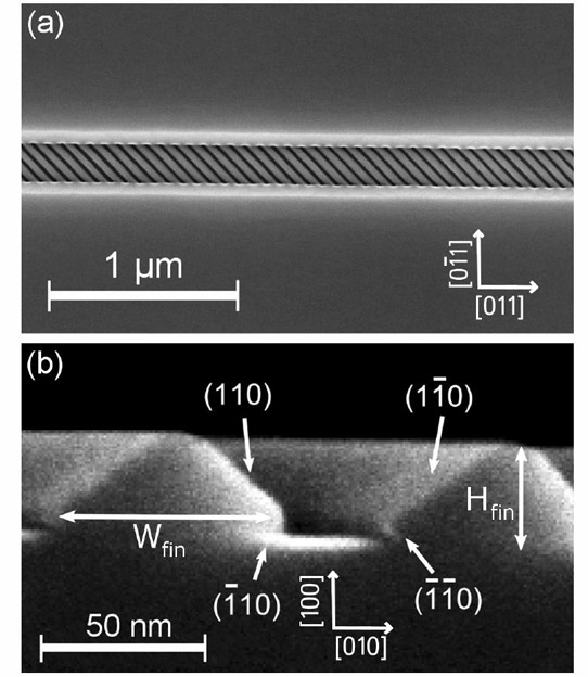
Figure 2: (a) Scanning electron micrograph (SEM) of device after second re-growth step. Shown are fins constituting the channel, as seen through the gate-opening in sacrificial InP and highly doped InGaAs contact layers. (b) Cross-sectional SEM of 60nm-wide fin, with crystal planes denoted.
A long gate length of 200nm allowed the device structure to achieve a low subthreshold swing (SS) of 85meV/decade and drain-induced barrier lowering (DIBL) of 88mV/V at 0.05V drain bias. At the higher 0.5V drain bias, the SS increased to 103mV/dec. The on/off ratio within a 0.5V window at 0.5V drain with 100nA/μm off-current was 1.5x10³. The SS for a 32nm gate length was 185mV/decade at 0.5V drain.
Radio-frequency measurements between 40MHz and 67GHz gave a cut-off frequency (fT) estimate of 210GHz and maximum oscillation (fmax) of 250GHz; “the highest of any reported III-V multiple-gate MOSFET, though below the records for planar III-V MOSFETs”, according to the researchers. The good performance is attributed to suppressed parasitic gate capacitance.
The poor SS in the short-channel/gate-length devices could be improved by etching the underlying InP to create gate-all-around structures or by using InAlAs back-barriers to reduce leakage effects.
III-V multiple-gate MOSFETs MOSFETS InP InP substrates MOVPE ALD Electron-beam lithography
http://ieeexplore.ieee.org/xpl/articleDetails.jsp?arnumber=6739081
The author Mike Cooke is a freelance technology journalist who has worked in the semiconductor and advanced technology sectors since 1997.


