


- News
28 March 2014
Distributed Bragg reflectors for InGaN LEDs on silicon
Sun Yat-sen University in China has improved the wall-plug efficiency of indium gallium nitride (InGaN) light-emitting diodes (LEDs) grown on silicon by incorporating a distributed Bragg reflector (DBR) [Yibin Yang et al, Appl. Phys. Express, vol7, p042102, 2014].
Although the growth of nitride semiconductor LED structures on silicon promises production cost benefits, there are two technical barriers to be overcome. First, the growth of high-quality gallium nitride on silicon is more difficult than on alternative, more expensive substrates such as sapphire or silicon carbide. Second, light emitted into the silicon substrate is lost because its bandgap is narrower than that of the overlying active nitride semiconductor structures.
One way to avoid the second problem is to remove the silicon substrate from the LED layers. However, such techniques are complicated and result in low yields and high cost. Incorporating a DBR between the silicon substrate and active light-emitting layers avoids the need to remove the substrate by reflecting the light upwards through the wide-bandgap layers that do not significantly absorb the produced photons.
The Sun Yat-sen University epitaxial nitride semiconductor layers (Figure 1) were grown on 2-inch n+-silicon (111) substrates in a Thomas Swann close-coupled showerhead metal-organic chemical vapor deposition (MOCVD) system.
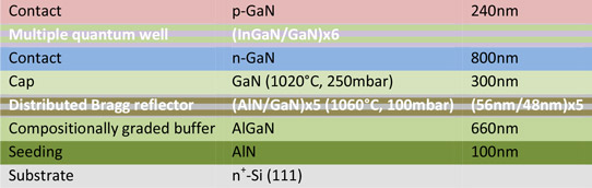
Figure 1: Epitaxial structure of LEDs with DBR.
The substrate was cleaned before deposition to remove surface oxidation. The 100nm aluminium nitride (AlN) nucleation/seeding layer was formed by first depositing aluminium and then introducing ammonia, preventing the formation of silicon nitride.
The AlN layer was also designed to prevent melt-back etching that occurs in the presence of gallium-silicon alloys. The next linear compositionally graded AlGaN layer was constructed to compensate for tensile stress and thus avoid cracking in the overlying layers.
The researchers found that the AlN/GaN DBR layers reduced the threading dislocation density significantly, compared with that of the underlying AlGaN and AlN.
The LED devices (Figure 2) were fabricated with through-hole connections to the n-contact layer using inductively coupled plasma reactive-ion etching (ICP-RIE). First, the n-GaN contact layer was exposed in a mesa etch. Further selective ICP-RIE drilled the holes down to the conductive n+-Si substrate.
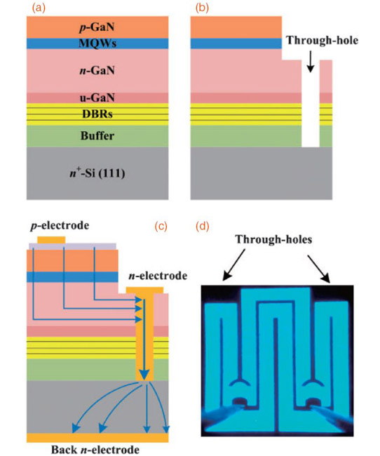
Figure 2: Fabrication processes of vertical-conducting DBR-based LED chips with through-holes: (a) epitaxial layer deposited on Si substrate; (b) dry etching to expose n-GaN and form through-holes; (c) depositing metals as electrodes and current paths of vertical-conducting DBR-based LED with through-holes marked by curves with arrows. (d) Light-emitting image of the vertical-conducting DBR-based LED chip with through-holes at an injecting current of 100mA.
The structure was then subjected to a 700°C anneal in nitrogen for 25 minutes to activate the magnesium-doping of the p-GaN contact. The researchers say that the annealing also partially repaired etch damage from the ICP-RIE process.
The p-GaN contact was covered with nickel/gold as a transparent conductor. Annealed chromium/palladium/gold was used as bonding pads for the p- and top n-electrodes. The same metal combination was used to fill the through-holes and thus short out the resistive DBR and AlGaN buffer layers.
The Si substrate was thinned to 100μm and was coated with titanium/nickel/gold as a back-side n-electrode. The resulting LED structure measured 1mm x 1mm.
The peak reflectance of the DBR was 58% at 463nm, significantly short of the theoretical value of 83%. The researchers write: “This difference may result from structural imperfections such as deviations from the designed layer thickness and interface roughness between each epitaxial layer. Scattering loss and absorption in the film are other potential causes.”
Even so, the photoluminescence was “significantly greater for the DBR-based LED”, compared with a device without DBR. The full-width at half-maximum (FWHM) of the peak was 8.6nm with DBR, but 17.6nm without. The researchers attribute the narrower line-width to “higher light efficiency and better crystalline quality owing to reflectivity enhancement and suppression of dislocation formation by the DBRs”.
The main peak for electroluminescence fell within the range 465-468nm for injection currents from 50mA up to 600mA.
The forward voltage at 20mA was 3.68V when the n-contact was made with the ‘lateral’ top n-GaN electrode and 3.96V when made with the bottom ‘vertical’ n-Si electrode. The corresponding series resistances were 5.5Ω and 7.7Ω. The greater series resistance with the vertical conduction scenario was attributed to the resistances of the top and bottom contacts with the silicon substrate and its bulk resistivity.
Without the through-hole structure, vertical conduction is limited with a current of 1.3μA even at 100V, giving a series resistance of the order of 107Ω. This reflects the insulating nature of the AlN seed, AlGaN buffer, and DBR layers.
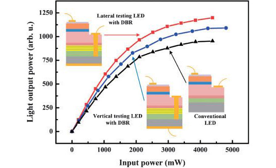
Figure 3: Light output power versus input power of DBR-based LEDs with through-holes under lateral and vertical testing modes, and conventional LED.
The wall-plug efficiency (WPE) for light output power of devices with DBRs for 2100mW input (350mA) increased by around 24% over the performance of conventional LEDs without DBRs (Figure 3). The DBR LEDs in the vertical conducting mode suffered from the higher series resistance, particularly at higher input power where self-heating effects led to performance degradation. Even so, the vertical DBR LED mode had greater WPE than conventional LEDs without DBRs.
Distributed Bragg reflectors DBR LEDs InGaN MOCVD GaN AlN
http://iopscience.iop.org/1882-0786/7/4/042102/article
The author Mike Cooke is a freelance technology journalist who has worked in the semiconductor and advanced technology sectors since 1997.


