


- News
20 March 2014
GaN-on-Si enabling GaN power electronics, but to capture less than 5% of LED making by 2020
Gallium nitride (GaN)-on-sapphire is the existing mainstream technology for LED manufacturing, but GaN-on-silicon technology has naturally appeared as an alternative to sapphire in order to reduce cost. However, a cost simulation by market analyst firm Yole Développement indicates that the differential in silicon substrate cost is not enough to justify the transition to GaN-on-Si technology. The main driver is the ability to manufacture on 6” or 8” wafers in existing, depreciated CMOS silicon fabs, according to the firm’s new report ‘GaN-on-Si Substrate Technology and Market for LED and Power Electronics’, which reviews GaN-on-Si technology growth, challenges and solutions.
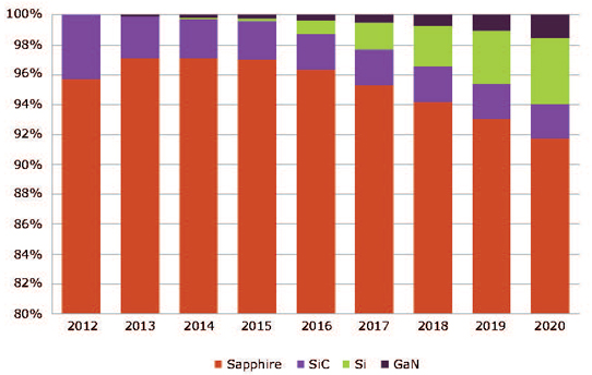
Picture: Penetration rate of various LED substrates.
Despite potential cost benefits for LEDs, the mass adoption of GaN-on-Si technology for LED applications remains unclear. Opinions regarding the chance of success for LED-on-Si vary widely in the LED industry from unconditional enthusiasm to unjustified scepticism, says Yole. Almost all major LED makers are researching GaN-on-Si, but few have made it core to their strategy and technology roadmap. Among the proponents, only Lattice Power, Plessey and Toshiba have moved to production and are offering commercial LED-on-Si.
Yole believes that, although significant improvements have been achieved, there are still some technology hurdles to be overcome (performance, yields, CMOS compatibility). “We consider that, if the technology hurdles are cleared, GaN-on-Si LEDs will be adopted by some LED manufacturers, but will not become the industry standard,” the firm says. “We expect that silicon will capture less than 5% of LED manufacturing by 2020.”
GaN-on-Si to be widely adopted for power electronics
The power electronics market addresses applications such as AC-to-DC or DC-to-AC conversion, which is always associated with substantial energy losses that increase with higher power and operating frequencies. Incumbent silicon-based technology is reaching its limit and it is difficult to meet higher requirements, says Yole. GaN-based power electronics have the potential to significantly improve efficiency at both high power and high frequencies while reducing device complexity and weight. Power GaN is therefore emerging as a substitute to silicon-based technology. However, currently power GaN remains at an early stage and represents just a tiny portion of the power electronics market.
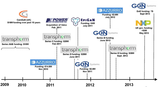
Picture: Recent M&A, investments and fund raisings in the GaN area.
“We are quite optimistic about the adoption of GaN-on-Si technology for power GaN devices,” says Yole. GaN-on-Si technology has brought to market the first GaN devices. In contrast to the LED industry, where GaN-on-sapphire is main stream and presents a challenging target, GaN-on-Si will dominate the GaN-based power electronics market because of its lower cost and CMOS compatibility, adds the firm. Although GaN-based devices remain more expensive than Si-based devices today, the overall cost of GaN devices for some applications is expected to be lower than silicon devices three years from now, according to some manufacturers.
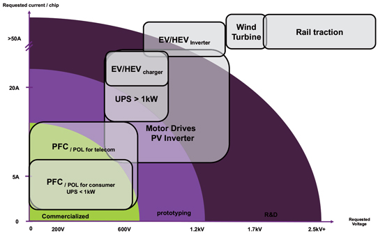
Picture: 2013 GaN device state of the art (V & amp) vs application requests.
“In our nominal case, GaN-based devices could reach more than 7% of the overall power device market by 2020,” forecasts Yole. GaN-on-Si wafers will capture more than 1.5% of the overall power substrate volume, representing more than 50% of overall GaN-on-Si wafer volume, subject to the hypothesis that 600V devices will take off in 2014-2015.
GaN-on-Si epi: buy it or make it?
To adopt GaN-on-Si technology, device makers have a choice between buying epiwafers or templates on the open market or buying metal-organic chemical vapour deposition (MOCVD) reactors and making epiwafers themselves. Today, there is a limited number of players selling either epiwafers or templates or both on the open market. These players comes from Japan, US and Europe. “We have not observed an absolute dominance from one region,” says Yole.
As perceived by device makers, each business model has its pros & cons in terms of intellectual property (IP), technology dependence, R&D investments, and time. “According to our analysis, we do not expect to see a significant template/epiwafer business emerge for LEDs, and consider that LEDs makers would prefer making their epiwafers internally for mass production,” says Yole. For the power electronics industry, opinion is divided, it adds. “We consider that buying epiwafers could work as long as the price of the epiwafer on the open market keeps decreasing,” the market research firm concludes.


