- News
9 May 2014
Beryllium oxide interlayer reduces interface trapping in InGaAs MOSFETs
Researchers based in USA and South Korea have developed a gate stack for III-V quantum well metal-oxide-semiconductor field-effect transistors (QW MOSFETs) based on a bilayer dielectric of beryllium oxide (BeO) and hafnium dioxide (HfO2) [D.Koh et al, Appl. Phys. Lett., vol104, p163502, 2014].
BeO has a large energy bandgap of 10.6eV and a larger conduction band offset from indium gallium arsenide (InGaAs) channel material than alternatives such as aluminium oxide (Al2O3). Such properties as exhibited by BeO are attractive for avoiding interface traps that adversely affect MOSFET performance. Other attractions of BeO include a ‘self-cleaning effect’, higher thermal stability, and better performance as an oxygen diffusion barrier.
The US/Korea research involved University of Texas at Austin, USA; SEMATECH Inc, USA; Chungnam National University, South Korea; GLOBALFOUNDRIES, USA; and Texas State University, USA.
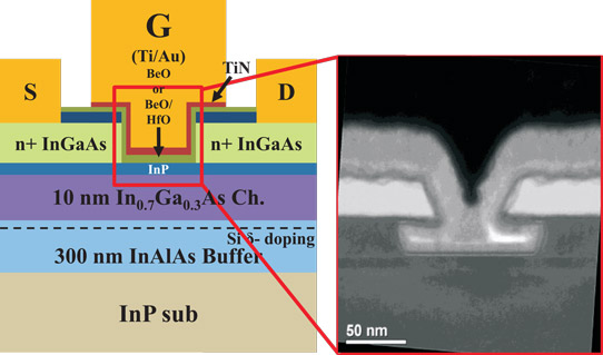
The III-V epitaxial structure was grown using molecular beam epitaxy (MBE) on indium phosphide (InP) substrate (Figure 1). The indium aluminium arsenide (In0.52Al0.48As) buffer provided a back-barrier for the indium gallium arsenide (In0.7Ga0.3As) quantum well. The final layers consisted of 2nm InP and 20nm n+-In0.53Ga0.47As. The n+-InGaAs reduced the access resistance to the channel and increased channel electron concentration.

Figure 1: Schematic of QW MOSFETs device structure with BeO or BeO/HfO2 as gate dielectric.
Transistor fabrication consisted of electrical isolation with a phosphoric acid wet etch, molybdenum/titanium/gold source/drain deposition, and gate stack formation. The patterning for the gate created a hard mask of silicon dioxide. The mask was used as the pattern for an etch down to the InGaAs cap with carbon tetrafluoride plasma, followed by phosphoric acid-based wet etch to the InP layer.
The BeO interface passivation and HfO2 dielectric (1nm/1.5nm) were applied using 250°C atomic layer deposition (ALD) in a Cambridge Nano system. The gate metal was titanium and the gate contact pad was titanium/gold.
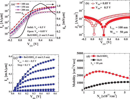
Measurements on MOS capacitors with a BeO/HfO2 bilayer gave a mid-gap interface trap density of 1x10¹²/eV-cm2. A 2nm BeO dielectric gave a higher density of 2x10¹²/eV-cm2. HfO2 on its own, or with Al2O3 interlayer, tends to produce higher values.
With 100nm gate length, the MOSFET achieved peak transconductance of 1.1mS/μm at 0.5V drain bias (Figure 2). The subthreshold swing was 100mV/decade, which is described as “excellent” by the researchers. The drain-induced barrier lowering was 100mV/V. The gate leakage current density was ~10−2A/cm2. At 0.6V gate potential, the drive current density was 0.35mA/μm.

Figure 2: Electrical characteristic of QW MOSFETs with BeO/HfO2 (1/1.5nm) gate stack. (a) Subthreshold performance with different channel length and transconductance (gm) of 100nm gate-length device, (b) gate leakage current density of 100nm device, (c) drive current of 100nm QW MOSFET, and (d) mobility enhancement of 10μm-gate 1nm/1.5nm BeO/HfO2 over 2nm BeO QW MOSFET.
The equivalent oxide thickness of the BeO/HfO2 bilayer stack was 0.93nm. Long-channel effective mobility was 2500cm2/V-s.
“These results highlight the potential of atomic-layer-deposited BeO for use as a gate dielectric or interface passivation layer for III–V MOSFETs at the 7nm technology node and/or beyond,” the researchers comment.
InGaAs MOSFETs QW MOSFETs InGaAs ALD
http://dx.doi.org/10.1063/1.4871504
The author Mike Cooke is a freelance technology journalist who has worked in the semiconductor and advanced technology sectors since 1997.


