- News
5 November 2014
Hot holes for improved injection into nitride LEDs
Researchers based in Singapore and Turkey have been developing a hole accelerator structure with a view to improving the performance of indium gallium nitride (InGaN) semiconductor light-emitting diodes (LEDs) [Zi-Hui Zhang et al, Appl. Phys. Lett., vol105, p153503, 2014]. The team was based at Nanyang Technological and Bilkent universities.
The aim of the hole acceleration structure was to improve hole injection over aluminium gallium nitride (AlGaN) electron-blocking layers (EBLs). The purpose of EBLs is to avoid electrons from overshooting the active multiple quantum well (MQW) light-emitting regions. Overshooting electrons end up recombining in the p-type hole injection layers, generally non-radiatively, reducing output power and efficiency.
However, EBLs also inhibit hole injection into the MQW, particularly since hole transport and density levels are lower than for electrons. The mobility for holes in p-GaN is typically less than 10cm2/V-s. By contrast, electron mobility in GaN is around 440cm2/V-s.

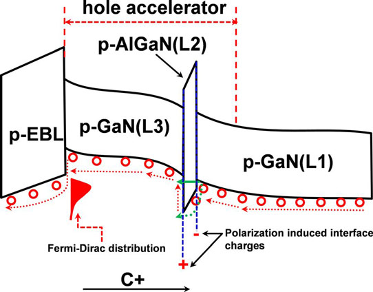
Figure 1: Schematic energy diagram of hole accelerator. Solid green and dashed green arrows illustrate the hole transport through intra-band tunneling and thermionic emission, respectively.
The team therefore designed a structure (Figure 1) that would accelerate holes and allow more to cross the EBL and reach the MQW. The p-type GaN hole injection region was divided in two by a thin layer of p-AlGaN. The AlGaN divider had to be thin to avoid hole blocking.
Polarization-induced AlGaN/GaN interface charges created an electric field in the region up to the EBL that accelerated holes over the barrier and into the MQW. The researchers worked with both simulations and actual LED structures.

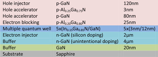
Figure 2: Epitaxial structure for LED B with hole acceleration structure.
The epitaxial structures were grown on c-plane sapphire through metal-organic chemical vapor deposition (MOCVD) – see Figure 2. LED structures with (LED B) and without (LED A) hole accelerator layers were grown after the electron-blocking p-type aluminium gallium nitride (AlGaN) layer (EBL). The device without hole acceleration had 200nm p-GaN after the AlGaN EBL. Bis(cyclopentadienyl)magnesium (Cp2Mg) was used as the precursor for the magnesium doping for the p-type layers.

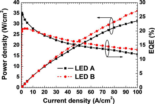
Figure 3: Experimentally measured optical output power density and EQE as function of injection current density for LEDs A and B.
The output power (Figure 3) of the LED B with hole acceleration had 15% higher output power density (36.1W/cm2) at 100A/cm2 current density, compared with LED A (31.4W/cm2). The droop at 100A/cm2 from maximum external quantum efficiency (EQE) was 54.2% for LED A and 35.9% for LED B. As is usual in such cases, the improvement in efficiency droop from the hole acceleration structure is not as dramatic as these figures suggest – the peak EQE of LED A is somewhat higher than that of LED B. A crossover in EQE occurs at around 20A/cm2.
The researchers comment: “The unimproved optical performance for LED B at the low current injection levels (<10A/cm2) is most likely due to the blocking effect by the p-Al0.25Ga0.75N layer in the hole accelerator region.”
http://scitation.aip.org/content/aip/journal/apl/105/15/10.1063/1.4898588
The author Mike Cooke is a freelance technology journalist who has worked in the semiconductor and advanced technology sectors since 1997.


