


- News
11 November 2014
Reducing threshold current in 3μm laser diodes
Researchers in USA have reduced the threshold current for 3μm laser diodes on gallium antimonide (GaSb), claiming a two-fold improvement over the previous world record [Leon Shterengas et al, Appl. Phys. Lett., vol105, p161112, 2014].
The devices were developed by State University of New York at Stony Brook (SUNY) and Army Research Laboratory (ARL) based on previous work at Stony Brook, which combined two laser diode structures with a ‘cascade pumping scheme’ between the stages. The new work eliminated the spacing between the intermediate pumping region and the quantum wells (where photons are generated) to improve optical confinement.
The device materials were created using solid-source molecular beam epitaxy on GaSb substrates. The structures (Figure 1) used aluminium gallium arsenide antimonide (Al0.80Ga0.20As0.07Sb0.93) doped with tellurium and beryllium for n- and p-type cladding regions, respectively. The barrier and waveguide core layers consisted of unintentionally doped aluminium gallium indium arsenide antimonide (Al0.20Ga0.55In0.25As0.23Sb0.77).
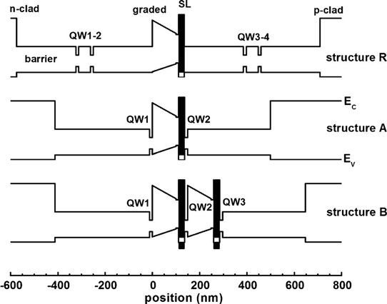
Figure 1: Schematic band diagrams of laser heterostructures under flat band condition. Structure R corresponds to Stony Brook’s previous cascaded laser diodes. Structures A and B correspond to two- and three-stage cascaded lasers designed for improved optical confinement and minimized threshold current density.
The quantum wells were 12nm layers of GaInAsSb with ~50% indium. The wells were compressively strained by 1.5%, compared with the rest of the heterostructure.
The cascade pump regions consisted of 100nm graded layers of AlGaAsSb with the aluminium fraction varying from 50% down to 5%, followed by tunnel junctions and electron injectors of 10nm GaSb, 2.5nm AlSb and 6-period chirped superlattice (SL) of tellurium-doped InAs/AlSb.
The materials were fabricated into 100μm- and 6μm-wide ridge laser diodes.
Three structures were studied – a reference device (structure R) from the previous work, a two-stage cascade diode with increased optical confinement (structure A), and a three-stage cascade design aimed at high efficiency, low threshold current and reduced voltage drop (structure B).
A 100μmx2mm anti-reflection and high-reflection (AR/HR) coated laser diode based on structure A achieved in continuous wave (CW) operation at 17°C a threshold current density of 100A/cm2, maximum power of 650W, and peak power conversion efficiency of 16% (Figure 2). The efficiency “remained well above 10% for output powers above ~600mW”, the researchers write, adding: “All of these characteristics surpassed those of the previous state-of-the-art 3μm lasers (i.e. reference structure R)”. In particular, the threshold was a factor of two smaller than that of the reference device. A 6μm-wide device demonstrated CW emission power above 100mW and power conversion efficiency ~10%.
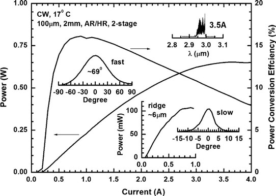
Figure 2: CW light-current-power conversion characteristics measured at 17°C for 100μm-wide, 2mm-long AR/HR coated two-stage cascade lasers. Insets show laser spectra at maximum power level, fast-axis far-field pattern as well as CW light-current characteristics of 2mm-long, AR/HR coated narrow (6μm) ridges with corresponding slow-axis far-field pattern.
Diodes with a 100μmx2mm ridge based on structure B with AR/HR coating were tested at 17°C and 70°C. The CW output power at 17°C reached 830mW (100mW at 70°C). Lengthening the ridge to 3mm increased the output power to 960mW. The increase is attributed to an improved thermal footprint. The hoped-for reduction in threshold current was not realized.
The researchers comment: “We hypothesize that this results from the barrier energy asymmetries pushing the electron envelope wave-functions in QW2 of Structure B toward the SL side and thereby intensifying adverse interface interactions”. Growth-to-growth variation effects on carrier localization and lifetimes could also have contributed to the higher-than-desired threshold current.
http://dx.doi.org/10.1063/1.4900506
The author Mike Cooke is a freelance technology journalist who has worked in the semiconductor and advanced technology sectors since 1997.


