


- News
18 November 2014
Staircase quantum barriers to improve LED efficiency at high current
Researchers based in China have found “remarkably reduced efficiency droop” from staircase (SC) thin indium gallium nitride (InGaN) quantum barrier (QB) light-emitting diodes (LEDs) [Kun Zhou et al, Appl. Phys. Lett., vol105, p173510, 2014]. The 200A/cm2 droop for a SC-QB LED was just 3.3% from the peak value. The light output power for the SC-QB LED was 47% higher than for a thin QB device, also at 200A/cm2.
InGaN LEDs suffer from a fall-off of efficiency at high currents. Researchers have found that one particular problem in such devices is the poor injection of holes into the light-emitting multiple quantum well (MQW) region. The holes that do get into the MQW tend to be concentrated toward the p-GaN contact end of the device. Non-uniform concentration results in high-carrier-density regions where non-radiative Auger-like recombination mechanisms could sap efficiency.
Attempts have been made to improve hole injection into and distribution across the MQW by thinning the barriers between wells. These efforts have met with some success by other groups, but the team from Chinese Academy of Sciences’ Suzhou Institute of Nano-tech and Nano-bionics (with members also variously associated with Key Laboratory of Nanodevices and Applications and Suzhou Nanojoin Photonics Co Ltd) did not find any significantly improved droop behavior by thinning barriers.
Instead, the researchers used a design with quantum barriers that changed in composition so that the barrier height varied between the various wells in a staircase-like manner to encourage more uniform hole distributions.
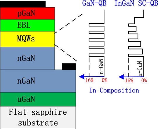
Figure 1: Schematic diagrams of LEDs with thin GaN-QBs and InGaN SC-QBs.
The LED structures (Figure 1) were grown on flat (0001) c-plane sapphire using metal-organic vapor phase epitaxy. The buffer consisted of 30nm low-temperature GaN nucleation and 1μm unintentionally doped uGaN layers. The nGaN contact layer was 4μm thick. The electron-blocking layer (EBL) was 20nm aluminium gallium nitride (pAl0.2Ga0.8N). The pGaN contact layer was 120nm.
The multiple quantum well (MQW) light-emitting active region consisted of either a standard 5-period In0.16Ga0.84N/GaN or In0.16Ga0.84N/InxGa1-xN well/barrier structure. The wells were 2.5nm, while the barrier thickness and composition was varied.
MQWs with In0.16Ga0.84N/GaN structure had barriers in the range 3nm-6nm. Standard 450nm LEDs often have thicker barriers of more than 10nm.
The staircase quantum barriers (SC-QBs) in the In0.16Ga0.84N/InxGa1-xN MQWs were fixed in thickness at 5nm. The SC-QB indium composition was varied between 2% and 10% (0.02-0.10) in steps of 2% from the nGaN to pGaN ends of the structure.
The researchers also produced samples with ‘monitor wells’ of 480nm wavelength replacing one of the 450nm wells. The aim of the monitor wells was to gauge the success in improving hole transport through the structure.
The epitaxial material was annealed to activate the magnesium doping of the p-type layers. Standard LED fabrication resulted in 250μmx400μm chips. The p-contact included an indium tin oxide (ITO) transparent electrode layer.
The devices with thin GaN QBs demonstrated similar droop behavior with the best external quantum efficiency (EQE) for the thickest barrier of 6nm under pulsed operation (20μsecs). For 3-6nm barriers the peak efficiency occurred in the range 15-24A/cm2. The droop from maximum at 200A/cm2 was in the range 23-30.6%. The smaller droop was from the 3nm device, but this was more the result of having a lower peak EQE.
The thinner barriers also reduced the blue-shift of the peak wavelength with increasing current, possibly due to smaller (strain-dependent) piezoelectric fields in the wells, according to the researchers. Thick quantum barriers impose the lattice constant of GaN more rigidly on the intervening wells.
Thin barriers should improve tunneling of holes and, since the droop is not significantly improved, the researchers conclude that tunneling is not the main mechanism for hole transport in thin GaN-QB LEDs.
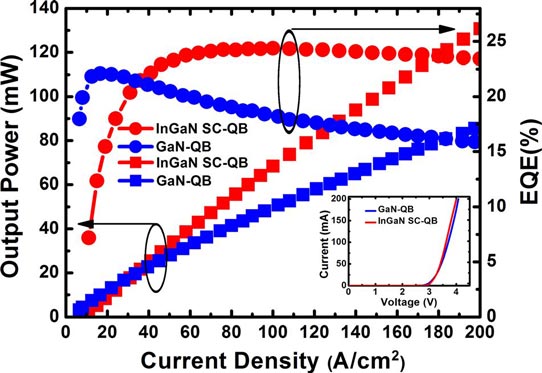
Figure 2: Electroluminescence output power and EQE as function of injected current density for GaN-QB and InGaN SC-QB LEDs. Inset: corresponding current-voltage curves.
The researchers then compared a 5nm thin GaN QB LED with a SC-QB device (Figure 2, Table 1). The SC-QB LED performs better when the current injection increases beyond 35A/cm2. While the thin QB LED EQE peaks at 22.1A/cm2, the maximum for the SC-QB device occurs at 95.1A/cm2.
Table 1: Power and efficiency values.
| Device | Injection current density | Output power | EQE |
| GaN-QB LED | 20A/cm2 | 12.0mW | 22.0% |
| InGaN SC-QB LED | 20A/cm2 | 9.0mW | 16.4% |
| GaN-QB LED | 100A/cm2 | 50.0mW | 18.3% |
| InGaN SC-QB LED | 100A/cm2 | 68.4mW | 24.4% |
The 200A/cm2 droop values were 28.4% and 3.3% for the thin QB and SC-QB devices, respectively. The light output power for the SC-QB LED was 47% higher than for the thin QB device at 200A/cm2. The researchers attribute the improved droop to lower carrier densities in the individual wells of the SC-QB structure.
LEDs with monitor wells suggested that the thin QB devices had a steady descent in intensity from well 1 to well 5 (pGaN to nGaN end) for an injection current of 200A/cm2. Well 5 had an intensity that was a factor of 4.5 down on that of well 1.
With SC-QBs, the least intensity came from well 4, which was a factor of 1.7 down on well 1. The more uniform distribution of the light emission across the wells in the SC-QB supports the idea that the reduction in droop results from the holes more effectively penetrating the MQW structure, giving lower carrier density in the individual wells.
LEDs Staircase quantum barriers InGaN GaN Efficiency droop
http://dx.doi.org/10.1063/1.4901078
The author Mike Cooke is a freelance technology journalist who has worked in the semiconductor and advanced technology sectors since 1997.


