


- News
28 October 2014
RF performance of junctionless trigate GaN FETs
Researchers based in Korea and France have measured the first high-frequency performance of gallium nitride (GaN) junctionless trigate field-effect transistors (JL TGFETs) [Ki-Sik Im et al, Jpn. J. Appl. Phys., vol53, p118001, 2014]. The work enabled the team from Kyungpook National University, Gachon University, Samsung Electronics Co Ltd and Grenoble Polytechnic Institute to create the first RF models for such devices.
Unlike the usual structure for GaN transistors, the JL TGFETs used only epitaxial GaN rather than a heterostructure of gallium nitride and aluminium gallium nitride.
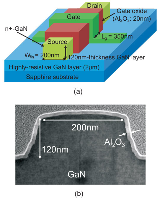
Figure 1: Device structure. (a) Schematic view. (b) Cross-sectional TEM image of fabricated GaN JL TGFET.
The junctionless (JL) trigate field-effect transistors (TGFETs) were fabricated on sapphire (Figure 1), based on a design presented and fabricated in 2013. The devices consisted of five fin channels in parallel. The maximum transconductance at -4.5V gate potential was 123.6mS/mm. The maximum drain current was 403mA/mm.
The threshold voltage of the device was -5.8V. Although these were depletion-mode normally-on transistors, the researchers believe that the more desirable enhancement-mode normally-off behavior could be achieved with suitable gate metals and device geometry.
With -4.5V gate potential and 10V drain bias, the cut-off (fT) and maximum oscillation (fmax) frequencies were 2.45GHz and 9.75GHz, respectively. These values are as-measured without de-embedding the effect of parasitic passive components.
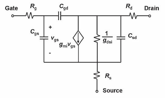
Figure 2: Small-signal equivalent circuit for extracting RF parameters from GaN JL TGFET in on-state.
The researchers also developed an RF model for the device (Figure 2, Table 1), which suggested that the source and drain resistances were about 100Ω. The team believes that “The model verification results and high-frequency performances of the GaN JL TGFET confirm its strong potential for application to RF ICs.”
Table 1: Summary of RF parameters extracted for GaN JL TGFET.
| Rg | 150.3Ω |
| Rs | 102.2Ω |
| Rd | 101.6Ω |
| gdsi | 58.5μS |
| gmi | 0.292mS |
| Cgs | 22.4fF |
| Cgd | 9.2fF |
| Csd | 15.5fF |
http://iopscience.iop.org/1347-4065/53/11/118001/
The author Mike Cooke is a freelance technology journalist who has worked in the semiconductor and advanced technology sectors since 1997.


