


- News
27 October 2014
Diamond transistor achieves 1530V breakdown voltage
Japan’s National Institute of Advanced Industrial Science and Technology (NAIST) has claimed the highest breakdown voltage to date for a diamond metal-semiconductor field-effect transistor (MESFET) [Hitoshi Umezawa et al, IEEE Electron Device Letters, published online 25 September 2014].
In principle, diamond transistors should benefit from high breakdown electric field, high thermal conductivity, low dielectric constant and high bulk carrier mobility. Such material properties could lead to high performance in terms of high-power and low-loss or high-power and high-frequency electronics.
High-temperature operation was also explored with a view to reducing or eliminating the need for complex and expensive thermal management.
The MESFETs were fabricated from microwave plasma-assisted chemical vapor deposition (MWCVD) p-type epitaxial material on semi-insulating Ib (001) synthetic diamond substrate (Figure 1). The carbon source was methane and the light p-type dopant was boron.
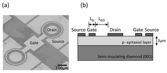
Figure 1: (a) Top view showing two linked diamond MESFETs with Corbino geometry and (b) cross-sectional schematic.
The researchers describe the boron doping as “unintentional” at the level of ~1015 atoms per cubic centimeter. The low doping level was aimed at preventing degradation of film quality and the Schottky contact.
The transistors were formed in circular ‘Corbino type’ configurations, with the ohmic drain contact in the center, the source contact on the outside, and the Schottky gate as a thin annulus between the source and drain. The ohmic metals were titanium gold.
The Schottky gate metal stack consisted of platinum/gold multi-layers. The gate region was exposed to ultraviolet light in ozone before the gate metal deposition. The pre-treatment was designed to give a stable oxygen termination of the surface bonds of the epitaxial layer.
The source-gate distance was fixed at 5μm. The gate length and gate-drain distance were varied to allow optimization of various performance characteristics.
The maximum drain current and peak transconductance of 20μm-gate-length devices (gate-drain 30μm) both increased as the temperature was raised from room temperature to 300°C. The drain currents were -0.06mA/mm and -1.23mA/mm, respectively. The corresponding transconductances were 9.7μS/mm and 61μS/mm. The increase in current is attributed to greater thermal activation of holes from the boron acceptor levels at 0.36eV (360meV >> 26meV gives low carrier density at room temperature). Another factor boosting the drive current, suggest the researchers, is lower ohmic contact resistance at high temperature.
Analyzing the parasitic resistances, the researchers extracted intrinsic values for the transconductance of 143μS/mm at 300°C (4.9x the value of 29μS/mm at room temperature).
The researchers say that improved current response would require reduced gate lengths, parasitic resistance in the source-gate gap, and ohmic contact resistance.
The threshold voltage of the device was 2.7V. The on/off current ratio was ~107 at room temperature, reducing to ~103 at 300°C. The much poorer ratio at 300°C was attributed to increased gate leakage (even under reverse bias) of the Schottky junction.
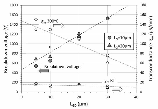
Figure 2: Breakdown voltage and transconductance of diamond MESFETs as a function of gate-drain distance (LGD) for gate lengths (LG) of 10μm and 20μm.
The breakdown was assessed with a 50V gate potential to reduce leakage currents. A number of 20μm-gate-length devices were tested (Figure 2). With a 30μm gate-drain distance, breakdown occurred at 1530V (2.5x higher than for a device reported in February 2014). The researchers claim the 1530V breakdown as “the highest for a diamond FET reported to date”. Previously, breakdown voltages in diamond transistors have been limited to less than 700V. The 1530V performance is almost comparable to that achieved in gallium nitride (GaN)-based devices.
After breakdown had occurred once, subsequent testing showed more than 30% degradation in breakdown voltage due to critical damage. Estimates of the critical electric field for breakdown were higher than the critical field for silicon, but were also 5-10x lower than the ideal value for diamond, suggesting room for improvement. One way to improve field profiles – reducing spikes and thus increase breakdown voltages – is to use field plates.
Diamond transistor MESFET Diamond
http://ieeexplore.ieee.org/xpl/articleDetails.jsp?arnumber=6910291
The author Mike Cooke is a freelance technology journalist who has worked in the semiconductor and advanced technology sectors since 1997.


