


- News
23 October 2014
First application of low-cost deposition of titanium dioxide for GaN MOS-HEMT
Researchers in Taiwan have used ultrasonic spray pyrolysis deposition (USPD) “for the first time” to apply titanium dioxide (TiO2) high-k dielectric layers to aluminium gallium nitride (Al0.25Ga0.75N/GaN) metal-oxide-semiconductor high-electron-mobility transistors (MOS-HEMTs) [Bo-Yi Chou et al, IEEE Electron Device Letters, published online 17 September 2014].
The team – from National Cheng Kung University, Feng Chia University, and Industrial Technology Research Institute – sees USPD as an economical deposition method. In particular, the non-vacuum process environment and high deposition rate make USPD suitable for low-cost large-area deposition and other mass-production scenarios.
USPD has previously been used to create aluminium oxide dielectric layers for GaN MOS-HEMTs. TiO2 has a higher dielectric constant of 86-173, compared with ~10 for aluminium oxide.
The epitaxial structure was grown using low-pressure metal-organic chemical vapor deposition (LP-MOCVD) on silicon (Figure 1). The MOS-HEMT fabrication involved mesa etching for electrical isolation, titanium/aluminium/gold deposition and annealing for ohmic source-drain contacts, 20nm TiO2 USPD for gate insulation, exposure of the source-drain electrodes, and nickel/gold deposition for the gate electrode. A reference Schottky-gate device was produced without TiO2 dielectric.
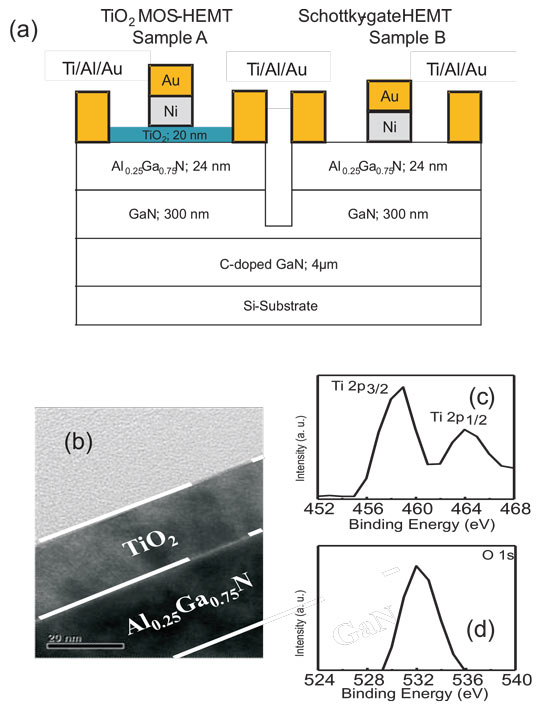
Figure 1: (a) Schematic diagram of AlGaN/GaN MOS-HEMT, (b) transmission electron microscope photo of MOS-gate structure, and (c) electron spectroscopy for chemical analysis (ESCA) intensities.
The gate length and width were 1μm and 100μm, respectively. The gate-source and gate-drain spacings were both 2μm.
Hall measurements before and after TiO2 USPD gave carrier densities of 2.08x10¹³/cm2 and 2.41x10¹³/cm2, respectively. The mobility slightly decreased, respectively, from 883cm2/V-s to 872cm2/V-s. The product of carrier density and mobility was increased from 1.84x10¹⁶/v-s to 2.1x10¹⁶/V-s, leading to expectations of increased on-current with TiO2 gate insulation/passivation.
Capacitance versus voltage (CV) measurement gave an oxide capacitance of 190pF and a dielectric constant (k) of 53.6, lower than the range quoted above. The composition of the USPD ‘TiO2’ was estimated as a Ti/O ratio of 0.47, which is slightly off the 0.5 for exact TiO2. The equivalent oxide thickness (EOT) of the 20nm TiO2 layer was estimated at 1.45nm.
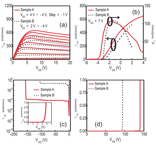
Figure 2: (a) Common-source IDS-VDS curves, (b) transfer gm/IDS, (c) two-terminal off-state IGD-VGD, and (d) BVDS characteristics at 300K.
Electrical performance between the devices was compared, generally showing improved performance of the MOS-HEMT over the Schottky HEMT (Figure 2, Table 1). The maximum drain current (IDS) of the MOS-HEMT was 650mA/mm. The peak transconductance (gm,max) was 107mS/mm. The reference Schottky HEMT had corresponding performance values of 511mA/mm and 110mS/mm. The increased gate-channel separation in the MOS-HEMT device only slightly decreased the peak transconductance due to use of TiO2 as a high-k dielectric with its 1.45nm EOT.
Table 1: Comparison of MOS-HEMT and Schottky HEMT.
| MOS-HEMT | Schottky HEMT | |
| Maximum drain current | 650mA/mm | 511mA/mm |
| Maximum drain current at 0V gate | 384mA/mm | 342mA/mm |
| Peak transconductance | 107mS/mm | 110mS/mm |
| Gate voltage swing | 2.7V | 1.7V |
| Two-terminal gate-drain breakdown voltage (BVGD) | -155V | -105V |
| On voltage | 3.8V | 1.8V |
| On-state breakdown (BVDS) | 139V | 94V |
| On/off current ratio | 4.5x10⁵ | 3.5x10² |
The gate voltage swing (GVS) linearity for transconductance within 90% of the peak value was 2.7V for the MOS-HEMT, compared with 1.7V for the Schottky HEMT.
The threshold voltage of the MOS-HEMT was negative (normally-on, depletion-mode) at -3.9V. At zero gate potential the maximum drain current (IDSS0) was 384mA/mm for the MOS-HEMT and 342mA/mm for the Schottky HEMT.
Table 2. Comparisons with other TiO2-dielectric MOS-HEMTs.
| Oxidation technique | USPD | Liquid phase deposition | Molecular beam epitaxy | Evaporation |
| Gate length | 1μm | 1μm | 0.7μm | 0.5μm |
| Dielectric constant, k | 53.6 | 24.4 | 70 | 80 |
| ΔIDSS0 | 12.3% | -7.8% | -6% | -67% |
| Δgm,max | -2.7% | -1% | -20.9% | -50% |
| gm, max | (110mA/mm) | (99mA/mm) | (140mA/mm) | (60mA/mm) |
| GVS (V) | 2.7V | 2.2V | 2V | 2.4V |
| IGD @ VGD -50V | 1x10⁻⁴mA/mm | 1x10⁻⁴mA/mm | 8x10⁻³mA/mm |
The researchers also compared their devices with those produced using different TiO2 deposition techniques (Table 2), commenting that USPD gave “the best improvement [over Schottky-based devices] of IDS at VGS = 0V (ΔIDSS0) of 12.3%, the highest GVS linearity of 2.7V, enhanced gm,max, and superior low IGD leakage.”
http://ieeexplore.ieee.org/xpl/articleDetails.jsp?arnumber=6901258
The author Mike Cooke is a freelance technology journalist who has worked in the semiconductor and advanced technology sectors since 1997.


