


- News
29 October 2014
Non-polar aluminium nitride growth for enhancing deep UV optoelectronics
North Carolina State University (NCSU) has been developing homo-epitaxy of non-polar aluminium nitride (AlN) with a view to deep ultraviolet (DUV, less than 300nm wavelength) optoelectronics [Isaac Bryan et al, J. Appl. Phys., vol116, p133517, 2014].
DUV light emission has been achieved using high-aluminium-content aluminium gallium nitride (AlGaN). However, the efficiencies are generally low due to high defect levels and unwanted electric fields that arise from the polarization of charge in the III-nitride chemical bond.
Defects arise in epitaxial material that has a large lattice-constant mismatch with the growth substrate. The effect of polarization can be reduced by choosing a crystal orientation where the electric fields are in the plane of the surface. Also, the polarization field can be increased by strain from lattice-mismatched hetero-epitaxy.
The NCSU research involved homo-epitaxy to eliminate lattice mismatching and growth on non-polar (1-100) m-plane substrates. This is in contrast to the conventional route to DUV light-emitting diodes grown in the (0001) c-plane direction on AlN templates on sapphire substrates.
The NCSU says of its work: “The growth of these high-quality non-polar AlN homo-epitaxial films will provide an ideal platform for future deep-UV optoelectronic device structures.”
Another potential advantage of m-plane material is that light extraction is expected to be higher compared with c-plane material due to non-propagation of TM-polarized photons along the c-direction (normal to the c-plane).
NCSU used AlN substrates created out of boules grown through physical vapor transport (PVT). The dislocation density of the boules was less than 103/cm3. A diamond wire saw was used to slice m-plane substrates from the c-plane boule. The substrate surface was smoothed using mechanical and chemical-mechanical polishing.
NCSU also implemented a wet etch/ammonia anneal treatment that the researchers have developed to reduce the total oxygen content of the substrate surface by more than 80%. Atomic force microscopy (AFM) of the substrate surface showed atomic-level steps. The root mean square (RMS) roughness of the substrate surface was “consistently” below 100pm for 5μmx5μm scan areas.
Epitaxial layers of 1.2μm AlN thickness were produced in a vertical cold-wall metal-organic chemical vapor deposition (MOCVD) reactor. The source gases were trimethyl-aluminium and ammonia in hydrogen carrier. The nitrogen/aluminium ratio was 1000. The growth temperature range and pressure were 1250-1550°C and 20Torr, respectively. Substrates with misorientation of 0.45° off [1-100] toward [0001] crystal direction were chosen for the epitaxial growth.
The surface of all the epitaxial layers “appeared smooth and featureless without cracking through optical differential interference contrast microscopy imaging,” according to the research team.
X-ray analysis gave rocking curve full-width at half maximum (FWHM) values between 18 and 25arcsec for the (10-10) peak along the [0001] direction.
The researchers comment: “These FWHM values are comparable to that of the substrates themselves, demonstrating that the epitaxial layers are of at least the same quality as the substrates. This demonstrates one advantage of using a high-quality native substrate.”
The symmetry of the x-ray peaks suggested the absence of strain between the epitaxial layer and substrate. Interference fringes in the curves from difference in carrier density (Pendellösung) suggested an abrupt change in free electron density between the substrate and epitaxial layer.
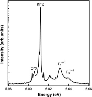 Figure 1: Low-temperature near-band-edge PL spectrum of a 1.2μm thick (1-100) homoepitaxial AlN film grown at 1450°C.
An epitaxial layer grown below 1350°C showed rough surfaces with RMS values of 8-13nm over 5μmx5μm areas. The surfaces also showed preferential faceting in the +/-[0001] direction. Above 1350°C the surface became atomically smooth, with RMS roughness of less than 0.4nm.
Photoluminescence on 1450°C material showed peaks from donor-bound (Si0X, 6.012eV) and free (Γ1, 6.032eV, Γ5, 6.040eV) excitons (Figure 1). There were also peaks from an oxygen bound exciton (O0X, 6.006eV), and two unidentified structures at 6.010eV and 6.003eV. The unidentified peaks are not typically seen in (0001) c-plane epitaxial films.
A two-step process with growth of 600nm at 1450°C followed by 600nm at 1350°C was used to study the impurity content through secondary-ion mass spectrometry (SIMS, Figure 2). The main effect of the higher growth temperature was to reduce the oxygen content by more than an order of magnitude. It was also found that the epitaxial layers had reduced silicon and carbon impurities compared with the substrate.
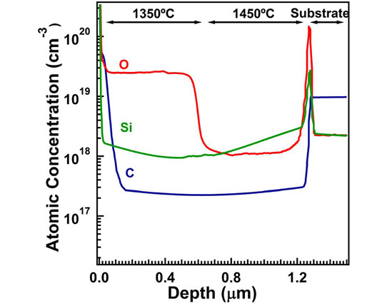
Figure 2: Calibrated SIMS depth profile for O, Si, and C in a two layer 1.2μm thick (1-1 00) homo-epitaxial AlN film with 600nm grown at 1450°C followed by 600nm grown at 1350°C.
The researchers compared the oxygen incorporation with 200nm (1-100) m-plane and (0001) c-plane films grown at 1250°C. The m-plane material had oxygen concentration of 4x10²⁰/cm3, compared with just 3x10¹⁷/cm2 for c-plane films.
The researchers comment: “It is clear from this SIMS analysis that (1-100) AlN homo-epitaxial growth at higher temperatures as compared to (0001) growth is necessary for high-purity epitaxial films, as the impurity incorporation depends on surface morphology.”
http://dx.doi.org/10.1063/1.4897233
The author Mike Cooke is a freelance technology journalist who has worked in the semiconductor and advanced technology sectors since 1997.


