


- News
7 October 2014
Diagonal quantum cascade transition improves photodetector performance
Vienna University of Technology in Austria has developed 8μm-wavelength quantum cascade (photo)detectors (QCDs) based on ‘diagonal’ transitions, resulting in almost an order of magnitude improved photocurrent response at room temperature [Peter Reininger et al, Appl. Phys. Lett., vol105, p091108, 2014].
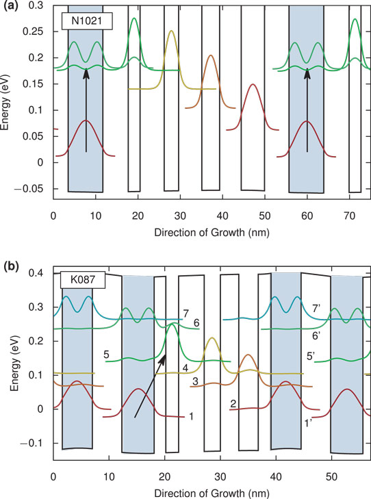
Figure 1: Band structure of quantum cascade designs with vertical (a) and diagonal (b) optical transitions, indicated by black arrows.
The researchers designed two cascade structures (Figure 1): a reference design with a conventional vertical transition within one well, and the other with a diagonal transition between adjacent wells. The team first performed simulations to show that the reduced optical coupling to the diagonal transition was compensated by improved electron extraction and reduced noise. The charge separation does not depend on resonant tunneling as in conventional vertical QCD structures, increasing extraction efficiency.
Also, the simulations suggested that the diagonal design is more robust with the potential for a wider range of devices to be developed for different wavelength detection. In the diagonal design, a 10% variation in the layer thicknesses led to only a 12% drop in response (peak wavenumber 1200/cm-1375/cm). By contrast, the vertical design was expected to have a lower response with a sharp decrease as the layers were thinned and the emission wavelength extended.
The robustness of the diagonal design could be of importance in other less intensively studied material systems where deposition methods are less mature, leading to wide variance of grown structures.
The InGaAs/InAlAs layers for the QCD were produced using molecular beam epitaxy (MBE) on indium phosphide substrate. A 30-period cascade structure was produced between silicon-doped InGaAs top (200nm) and bottom (600nm) contact layers. Mesa devices were fabricated with wet etching and deposition of germanium/gold/nickel/gold top and bottom contacts. The mesa devices were illuminated through a 45° polished facet.
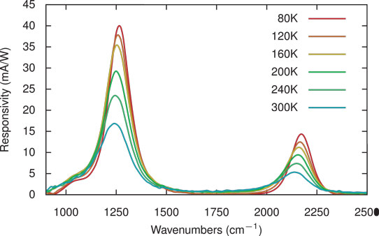
Figure 2: Measured photocurrent spectrum of diagonal transition QCD.
The photocurrent (Figure 2) from the diagonal QCD device showed two peaks at 1250/cm and 2150/cm wavenumbers (1/(wavelength). The room-temperature peak response was 16.9mA/W for 8μm wavelength (1250/cm wavenumber). This response is almost an order of magnitude better than for other reported 8μm-wavelength QCDs at room temperature.
The researchers attribute the main 1250/cm peak to a transition between levels 1 and 5 in the calculated band structure (Figure 1). The smaller 2150/cm peak is thought to arise from a transition between levels 1 and 6. A small bump at 1050/cm is explained as being due to a small overlap between levels 1 and 4.
Quantum cascade photodetectors InGaAs/InAlAs layers MBE
http://dx.doi.org/10.1063/1.4894767
The author Mike Cooke is a freelance technology journalist who has worked in the semiconductor and advanced technology sectors since 1997.


