


- News
8 October 2014
Cantilever bridge to higher bandwidth from VCSELs
Researchers at Japan’s Tokyo Institute of Technology and King Abdulaziz University in Saudi Arabia have developed a multiple-wavelength vertical-cavity surface-emitting laser (MW-VCSEL) array with a thermal wavelength drift of less than 0.017nm/K by the use of micro-electro-mechanical system (MEMS) cantilever structures to vary the cavity length [M. Nakahama et al, Appl. Phys. Lett., vol105, p091110, 2014].
The drift was 4x smaller than for conventional VCSELs, according to the researchers. With a channel spacing of 2.5nm, the devices could be operated over a 100K range without overlap.
The researchers see the devices as potential candidates for high-bandwidth optical data transmission based on wavelength division multiplexing (WDM) with application to warehouse-scale data centers and high-performance supercomputers. Traditional VCSELs allow only coarse WDM due to thermal wavelength drift. The researchers comment: “If the temperature dependence of wavelength is reduced, more channels are allocated in narrower spacing, resulting in larger transmission capacities.”
The team hopes that its technology could lead to narrow channel spacing, allowing bandwidths beyond 100 gigabits per second (Gbps).
The top distributed Bragg reflector (DBR) of each VCSEL in the array was sited on a cantilever (Figure 1). The cantilevers consisted of aluminium gallium arsenide (AlGaAs) of varying composition. The Al0.85Ga0.15 strain compensation layer had a smaller expansion coefficient compared with the AlGaAs DBR. The cantilevers were produced using a combination of selective wet etching and critical point drying.
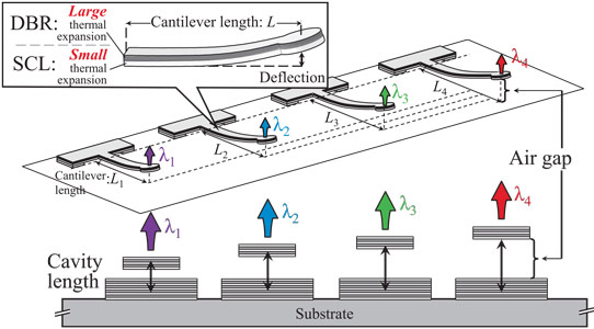
Figure 1: Design concept of 4-channel athermal multiple wavelength VCSEL array.
The researchers also used an aluminium oxide layer as an anti-reflection layer on the bottom half VCSEL to reduce Fresnel reflection effects at the interface between the semiconductor cavity and the air gap and to eliminate coupled cavity effects.
The thermal performance of the array was measured on a copper stage with a thermoelectric cooling element. At 20°C the maximum output power varied between 0.07mW and 0.22mW, while the threshold currents were in the range 1.2-1.5mA. The researchers hope that optimized fabrication would reduce the variations. In particular, the oxide apertures varied over the range 2-3μm. Smaller apertures result in lower output power.
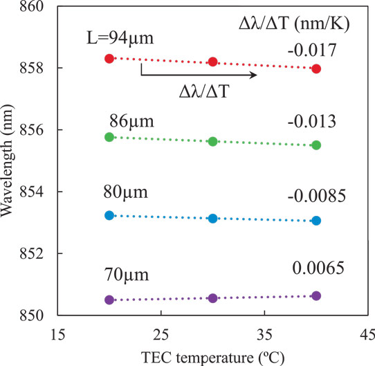
Figure 2: Peak wavelength of each device at different temperatures. Temperature coefficient of wavelength (Δλ/ΔT) was estimated from linear fit.
By varying the cantilever length between 70μm and 94μm, a wavelength span of 8nm at 20°C was achieved at 3mA injection. The devices showed single-mode operation with 30dB side-mode suppression ratio. However, at increased temperature, while the single-mode operation was maintained, the peak intensity decreased rapidly due to the poor temperature dependence of the threshold current as a result of the small aperture diameters. The thermal wavelength drift was between +0.0065nm/K and -0.017nm/K (Figure 2).
http://dx.doi.org/10.1063/1.4895337
The author Mike Cooke is a freelance technology journalist who has worked in the semiconductor and advanced technology sectors since 1997.


