


- News
13 October 2014
Color tuning from defect engineering
Xi’an Jiaotong University and Shaanxi Supernova Lighting Technology Co., Ltd., of China have used silver nanorods to engineer gallium vacancy defects in gallium nitride (GaN) to create color tunable light emitting diodes [Yaping Huang et al, Appl. Phys. Express, vol7, p102102, 2014]. At low current the emission was red, while at higher current white light was achieved.
The LED heterostructure was produced using metal-organic chemical vapor deposition on c-plane sapphire. The 460nm blue light-emitting region consisted of nine 3nm indium gallium nitride (InGaN) wells separated by 9nm gallium nitride barriers. The 120nm p-GaN contact region was separated from the multiple quantum well by a 20nm electron blocking layer.
The heterostructure was used to fabricate vertical LEDs (Figure 1). First 200nm-diameter polystyrene spheres were used as a self-assembled mask to create a hexagonal array of holes in a titanium hard mask. Before titanium deposition, the spheres were reduced in diameter to 130nm by oxygen plasma etching. The titanium mask therefore consisted of 130nm-diameter holes after removal of the polystyrene.
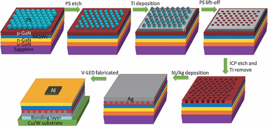
Figure 1: Fabrication scheme of defect-induced color-tunable vertical LEDs.
The titanium mask was used to create 130nm deep holes in the p-GaN contact layer. The titanium was then removed and 150nm silver deposited on a 1nm nickel layer. Further metal layers of 100nm titanium and 500nm gold was applied for subsequent bonding at 380°C to a copper/tungsten substrate with titanium/tin-gold alloy (50nm/1000nm) coat.
Laser lift-off was used to remove the sapphire growth substrate. The undoped GaN buffer layer was etched away before 1500nm aluminium was applied as contact metal to the n-GaN layer. The fabricated LED measured 55milx55mil (1.4mmx1.4mm).
One effect of the silver nanorod array is to create gallium vacancies in the p-GaN layer from formation of gallium-silver solid solution at the interface between the materials during thermal annealing/bonding.
At low injection current of 200mA, the emission is red with a peak at ~750nm (Figure 2). As the current increases, the broad emission blueshifts to ~650nm at 1600mA and broadens on the high energy side. The broad red emission is attributed to donor–acceptor pair (DAP) transitions in the p-GaN from electrons that successfully tunnel through the electron blocking layer. Above 600nm, a blue emission peak emerges around 470nm, presumably direct emission from the multiple quantum well structure.
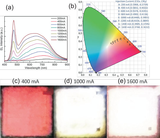
Figure 2: (a) Electroluminescence spectrum of vertical LEDs with silver nanorods embedded in p-GaN measured at room temperature under continuous current. (b) CIE (1931) chromaticity coordinates of vertical LEDs at various injection currents. Electroluminescence images of vertical LED chips at injection currents of (c) 400mA, (d) 1000mA, and (e) 1600mA.
The researchers characterize the color of LED as being red at 200mA and white at 1600mA on the basis of CIE 1931 chromaticity coordinates.
Current-voltage measurements gave a relatively high current leakage under reverse bias. The forward bias threshold for light emission was around 2V. The voltage at 200mA was 2.1V. At 600mA, the voltage was 2.9V where the MQW turns on.
The researchers admit that the efficiency of these devices are less than those of commercial phosphor-based white LEDs and that many improvements would be needed to boost efficiency in the future.
http://iopscience.iop.org/1882-0786/7/10/102102/
The author Mike Cooke is a freelance technology journalist who has worked in the semiconductor and advanced technology sectors since 1997.


