


- News
17 October 2014
Adoption of flip-chip LEDs and chip-scale packaging changing material/equipment market and supply chain
Following the LED TV crisis and with the entry of Chinese players, positioning has been reshuffled in the LED industry, according to the report ‘LED Packaging Technology and Market Trends 2014’ from Yole Développement. The quality of products from Chinese LED makers has increased to a level where they are now real competitors to all players, notes the market research firm. In such a highly competitive environment, three major challenges lie ahead for the LED industry regarding the general lighting market: improving efficacy, reducing cost, and increasing color consistency.
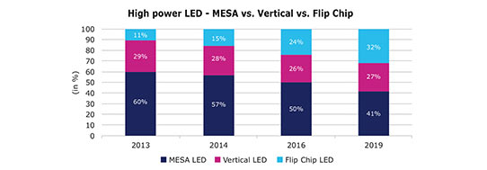
To answer these challenges, several players have now turned to flip-chip (FC) LEDs, which present several advantages over traditional horizontal (mesa) and vertical LEDs. These are wire-bonding free, can be driven at higher current, and have a smaller size package, notes Yole.
Also, although FC LED technology was launched quite a long time ago (by Lumileds), it was restricted from ‘popularization’ due to technical barriers (e.g. low yield regarding bumping/eutectic process). Additionally, the financial investment required (for packaging equipment) represented a strong barrier in an industry that was still recovering. However, the technology has gradually attracted attention from the lighting, backlighting and flash markets, becoming one the most important developing items in 2014.
Whereas flip-chip LED represented just 11% of overall high-power LED packaging in 2013, Yole expects this to rise to 34% by 2020. Flip-chip LEDs will take market share from vertical LED that will represent 27% of overall high power LED packages by 2020.
In addition to offering an increased ‘performance/cost’ ratio, flip-chip LEDs are also a key enabling technology for the development of chip-scale packages (CSP), which could allow further cost reduction.
CSPs are novel to the LED industry but they are the mainstay of the semiconductor industry. Development of CSPs for silicon ICs was driven by miniaturization, improved thermal management, higher reliability, and simply the need to connect to an ever increasing pin-count on an ever shrinking die. CSPs also enabled a reduction in device parasitics and allowed ease of integration into Level 2 packaging (e.g. module packaging for LEDs). It is therefore a natural evolution for this packaging innovation to proliferate into other industries (such as the LED industry).
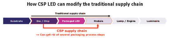
Basically, a CSP represents a single-chip direct-mountable package that is the same size as the chip. Regarding LED devices, CSPs are made of a blue FC LED die on which a phosphor layer is coated (the main application of such a package being general lighting). CSP presents several advantages (including miniaturized size and better thermal contact to substrates). However, eliminating several process steps of traditional LED packaging, CSPs are also having an impact on the industry structure, with some LED chip makers supplying their products directly to LED module makers. In the middle and long term, this technology could make chip makers supply directly to module makers.
Led packaging materials market to grow by 1.5x in 2014-2019, driven by package substrate, phosphor and encapsulant/optic material
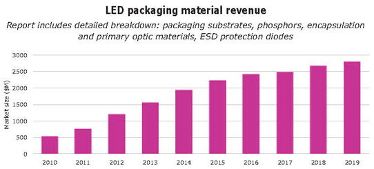
With the general lighting market triggered, LED packaging needs materials that meet the requirements of the applications. Regarding packaging substrates, the high power density of devices induces the use of ceramic substrates, a market that will grow from nearly $400m in 2013 to $700m in 2019. Encapsulant/optic materials will follow the same trend (from nearly $300m in 2013 to $700m in 2019), driven mostly by the increased use of silicone material offering better reliability/lifetime than traditional epoxy material. At the phosphor level, the expiry of key ‘yellow phosphor’ patents in this area from 2017 will increase the adoption of YAG (yttrium aluminium garnet) and increase competition (ultimately leading to further price decreases). But, even with the decrease in average selling prices (ASPs), the market will grow from nearly $600m in 2013 to $900m in 2019.
LED packaging equipment market growth to return for next 3 years, then fall sharply
The LED packaging equipment market, which stagnated in 2012 due to industry oversupply, is growing again but will peak at nearly $600m by 2015-2016, forecasts Yole. Indeed, the period 2013-2016 represents the main investment cycle for general lighting applications with the change of investment type due to flip-chip and chip-scale packages, adds the firm.
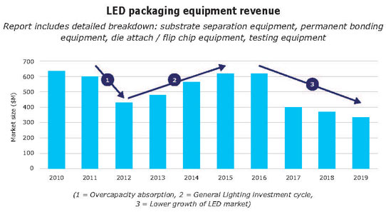
After 2016, the market will decline sharply for several reasons, two of which are the widely expected consolidation of the industry and the lower growth of the market. After 2019, it is questionable whether new LED applications (medical lighting, smart lighting etc) will impact the equipment market, concludes Yole.
www.i-micronews.com/led-report/product/led-packaging-technology


