


- News
10 September 2014
Aixtron partners with Fraunhofer IISB to enhance SiC production technology
Deposition equipment maker Aixtron SE of Aachen, Germany has teamed up with research institution Fraunhofer IISB (Institute for Integrated Systems and Device Technology) in Erlangen, Germany, to develop 150mm silicon carbide (SiC) epitaxy processes using Aixtron’s new 8x150mm G5WW vapor phase epitaxy (VPE) system. The Planetary Reactor tool will be installed at the IISB cleanroom laboratory in fourth-quarter 2014.
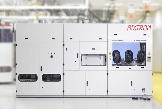
Picture: Aixtron’s new 8x150mm G5WW system.
“Through this partnership we expect to further accelerate the implementation of 150mm SiC technology in the industry by pairing our process know-how in manufacturing SiC epitaxial layers with Aixtron’s SiC equipment expertise,” comments Dr Jochen Friedrich, head of the Crystal Growth Department at Fraunhofer IISB. “We will use the G5WW production system for process optimization and demonstration purposes at the IISB facilities in Erlangen.”
Fraunhofer IISB has developed fundamental understanding in low-defect-density SiC epitaxial processes which are elementary for the manufacturing of high-voltage SiC devices. Special characterization techniques such as room-temperature photoluminescence imaging and selective defect etching have been developed and adapted to the SiC material properties. Also in Fraunhofer IISB’s laboratories complete SiC prototype devices can be processed and characterized.
“Based on the worldwide recognized experience of Fraunhofer IISB in SiC epitaxy technology and characterization, we will jointly enable the optimization of epitaxial production processes for 150mm SiC wafers using our state-of-the-art G5WW production tool,” says Dr Frank Wischmeyer, Aixtron’s vice president Power Electronics. “The goal of the collaboration is the demonstration of high-volume manufacturing processes addressing the SiC material requirements of SiC power devices,” he adds. “With this joint effort we support Aixtron customers worldwide moving from 100mm to 150mm SiC processing technology from the year 2015 to achieve efficient and economic manufacturing processes for future SiC power devices.”
Today, a variety of SiC devices like Schottky diodes and metal-oxide-semiconductor field-effect transistors (MOSFETs) are commercially available and put into practical use in switch mode power supplies (SMPS) for computer servers and TVs, in solar power inverters and efficient power converters in uninterruptible power supplies (UPS), medical equipment or commuter trains. To facilitate the widespread adoption of SiC in power electronics, cost reductions in SiC semiconductor material manufacturing and device processing are targeted through the implementation of 150mm SiC technology, says Aixtron.


