


- News
25 September 2014
GaN micro-rods grown on graphene yield flexible LEDs
Currently, most flexible electronic and optoelectronic devices are fabricated using organic materials. However, for these devices inorganic compound semiconductors such as gallium nitride (GaN) can provide advantages over organic materials — including superior optical, electrical and mechanical properties — but they are difficult to grow on flexible substrates.
Now, researchers at Seoul National University (SNU) led by professor Gyu-Chul Yi have grown GaN micro-rods on graphene to create transferrable LEDs and enable the fabrication of bendable and stretchable devices (Kunook Chung et al, APL Materials, 2, 092512 (2014)).
“GaN microstructures and nanostructures are garnering attention within the research community as light-emitting devices because of their variable-color light emission and high-density integration properties,” says Yi. “When combined with graphene substrates, these microstructures also show excellent tolerance for mechanical deformation.”
Ultrathin graphene films consist of weakly bonded layers of hexagonally arranged carbon atoms bound together by strong covalent bonds. This makes graphene an ideal substrate “because it provides the desired flexibility with excellent mechanical strength — and it's also chemically and physically stable at temperatures in excess of 1000°C,” says Yi.
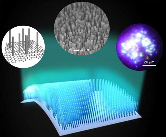
Picture: A rendering of the micro-rod growth process. Credit: Seoul National University.
For the GaN micro-rod growth, the very stable and inactive surface of graphene offers a small number of nucleation sites for GaN growth, which would enhance three-dimensional island growth of GaN micro-rods on graphene. To create the actual GaN microstructure LEDs on the graphene substrates, the team uses a catalyst-free metal-organic chemical vapor deposition (MOCVD) process that they developed in 2002. “Among the technique's key criteria, it is necessary to maintain high crystallinity, control over doping, formation of heterostructures and quantum structures, and vertically aligned growth onto underlying substrates,” Yi says.
When the team put the bendability and reliability of the GaN micro-rod LEDs fabricated on graphene to the test, they found that the resulting flexible LEDs showed intense electroluminescence (EL) and were reliable. “There was no significant degradation in optical performance after 1000 bending cycles,” notes Kunook Chung, lead author of the paper and a graduate student in SNU’s Physics Department. The researchers reckon that this represents a breakthrough for next-generation electronic and optoelectronic devices, enabling the use of large-scale and low-cost manufacturing processes.
“By taking advantage of larger-sized graphene films, hybrid heterostructures can be used to fabricate various electronics and optoelectronics devices such as flexible and wearable LED displays for commercial use,” concludes Yi.
http://scitation.aip.org/content/aip/journal/aplmater/2/9/10.1063/1.4894780


