


- News
16 September 2014
Ultrafast charge separation in metal dichalcogenide heterostructure
Researchers in USA and China have demonstrated “for the first time” efficient charge transfer in molybdenum/tungsten disulfide (MoS2/WS2) monolayer semiconductor heterostructures [Xiaoping Hong et al, Nature Nanotechnology, published online 24 August 2014]. The researchers from University of California at Berkeley, Lawrence Berkeley National Laboratory, Peking University, Arizona State University and Kavli Energy NanoSciences Institute say that the hole transfer time from the MoS2 to WS2 layer is ultrafast, at less than 50 femtoseconds (50x10-15 seconds or, more correctly, 5x10-14 seconds).
Metal dichalcogenides (MX2) such as MoS2 and WS2 form two-dimensional semiconductor structures with strong coupling to light fields, raising the prospect of optoelectronic and solar cell applications. Solar cells need efficient techniques to separate electrons and holes generated by incoming photons. The researchers see opportunities for photodetection, photovoltaics and photocatalysis arising from the combination of the demonstrated ultrafast charge transfer and strong optical absorption of MX2 semiconductors.
The researchers chose to study the MoS2/WS2 combination because previous theoretical work suggested that these materials would form a ‘type II’ band profile with the conduction band lowest in one material and the valence band highest in the other (Figure 1). With such an energy level structure, the electrons would congregate in the material with the lowest conduction band and the holes in the material with highest valence band (holes ‘float’ upwards in energy), hopefully enabling efficient separation for energy harvesting.
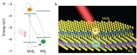
Figure 1: Band alignment and structure of MoS2/WS2 heterostructures. (a) Schematic of theoretically predicted band alignment of MoS2/WS2 heterostructure. (b) Illumination of MoS2/WS2 heterostructure with MoS2 monolayer lying on top of WS2 monolayer creates electron and hole in separate layers.
The MoS2 monolayer was grown on 285nm silicon dioxide on silicon substrate, using chemical vapor deposition (CVD). The WS2 monolayer was grown on sapphire, again with CVD. The WS2 material appeared on the sapphire substrate as flakes.
The MoS2 was transferred to the WS2 on sapphire on polymethyl methacrylate (PMMA) film. The film was spin coated on the MoS2 and released from the substrate by etching in potassium hydroxide solution. After transfer onto the WS2, the PMMA was dissolved in acetone.
The MoS2/WS2/sapphire was annealed to create the heterostructure. Raman spectroscopy was used to confirm that the heterostructure consisted of monolayers of MoS2 and WS2.
Photoluminescence with 2.33eV radiation at 77K on regions with only MoS2 or WS2 gave resonance peaks at 1.93eV or 2.06eV, respectively. The researchers attribute these resonances to A-excitons’ – bound states of electrons and holes. In regions where MoS2 overlaid WS2 to form a heterostructure, these peaks were significantly ‘quenched’. The researchers take this as evidence that charge transfer had taken place with the separation of the electrons and holes into the MoS2 and WS2 layers, respectively. An alternative quenching mechanism of energy transfer would by contrast reduce the high-energy peak and enhance the lower-energy peak, according to the researchers. The quenching effect was also seen in room-temperature measurements.
The researchers also carried out more detailed pump-probe experiments at 77K. The probe consisted of detecting changes in the reflection spectrum at various times after the pump pulse. By changing the energy of the pump photons the separate excitons could be generated. The researchers used a 1.86eV photon pump to generate MoS2 excitons. The change in reflection spectrum was directly proportional to the absorption spectrum.
Resonant features at 2.06eV and 2.46eV were found in the absorption spectra of MoS2/WS2 heterostructures. The researchers attribute these, respectively, to the A- and B-exciton states in WS2. Such features are not seen in WS2-only samples since the pump energy is too low to excite them. The researchers comment: “This provides direct evidence of efficient charge separation in photoexcited MoS2/WS2 heterostructures (Fig. 1a): electron–hole pairs are initially created in the MoS2 layer, but holes quickly transfer to the WS2 layer due to the type II band alignment, while electrons stay in the MoS2 layer.”
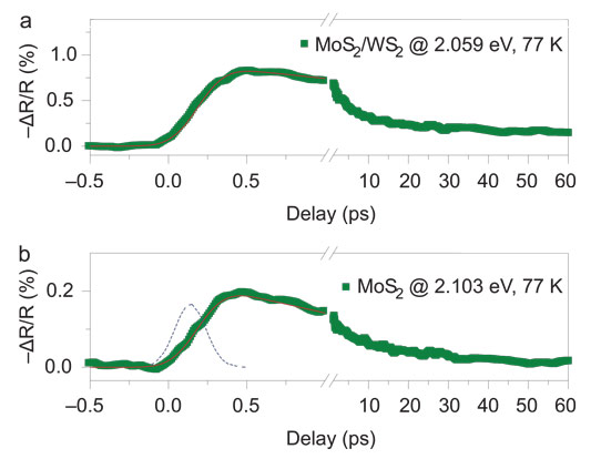
Figure 2: (a) Evolution of transient absorption signals at the WS2 A-exciton resonance in MoS2/WS2 heterostructure. (b) Dynamic evolution of transient absorption signals at the MoS2 B-exciton resonance in isolated MoS2 monolayer. Both signals show almost identical ultrafast rise times, limited by laser pulse duration of ~250fsecs. By convoluting instrument response function (blue dashed line in b) and instantaneous response in MoS2, reproduces ultrafast dynamics in MoS2 monolayer (red trace in b). Similar convolution shows that rise time in MoS2/WS2 monolayer is ∼25fsecs (red trace in a) and has upper limit of 50fsecs.
Using the rise time for the exciton resonance, the researchers estimate that the hole transfer occurs within 50fsecs of the pump pulse (Figure 2). “Similar ultrafast hole transfer also takes place at room temperature,” the researchers say. Most processes in MX2 materials, such as exciton lifetimes, are typically on the order of tens of picoseconds (10-12 seconds).
The researchers believe that the efficient charge separation is due in part to the formation of ‘charge transfer excitons’, with the electrons and holes binding across the interface between the different layers.
Metal dichalcogenide heterostructure CVD
www.nature.com/nnano/journal/v9/n9/full/nnano.2014.167.html
The author Mike Cooke is a freelance technology journalist who has worked in the semiconductor and advanced technology sectors since 1997.


