


- News
10 September 2014
Gallium arsenide on graphene/silicon substrate
Researchers in USA and Saudi Arabia have been exploring the potential of using ‘van der Waals epitaxy’ (vdWE) to grow gallium arsenide (GaAs) on silicon [Yazeed Alaskar et al, Adv. Funct. Mater., published online 26 August 2014]. The team consisted of personnel from the universities of California at Los Angeles (UCLA), Riverside and Irvine, and the Saudi Arabia National Nanotechnology Research Center.
Van der Waals epitaxy involves growth on two-dimensional (2D) layered materials such as graphene (Figure 1). In 2D-layered materials there are strong in-plane bonds and weak van der Waals bonds between the layers. Other 2D layered materials include molybdenum/tungsten sulfide/selenide. The researchers hoped that the use vdWE could alleviate the constraints of lattice and thermal expansion mismatch, etc.
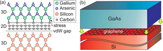
Figure 1: a) Atomic geometry of GaAs/multi-layer graphene/Si interface showing only top-most graphene layer is strained by heteroepitaxial growth, b) schematic for structure with GaAs grown on top of single-layer graphene buffer layer/Si substrate.
The researchers used a Perkin Elmer 430 molecular beam epitaxy (MBE) system to deposit the GaAs on a multilayer graphene buffer on silicon (111) substrate. The graphene consisted of flakes exfoliated using Scotch tape and transferred to the silicon. The surface was cleaned using acetone and isopropanol both before and after the graphene application. The researchers were keen to remove traces of organic materials from the exfoliation process.
Raman spectroscopy showed a low response for the disorder-induced D-band peak, which had an intensity ratio of less than 0.1 compared with the G-band peak. The Raman result suggests high-quality multi-layer graphene. Atomic force microscopy (AFM) gave a root mean square (RMS) roughness of 0.2nm.
The researchers tried two nucleation techniques. In the first, an arsenic-terminated surface was produced on which GaAs was then grown. In the second, the initial surface termination was changed to gallium.
The As-termination technique resulted in clumping of the GaAs into islands, leading to poor-quality GaAs. For Ga-termination, the research got the best results from two monolayers of Ga. The Ga pre-layer was deposited at room temperature. The first deposition of GaAs occurred at 350°C, avoiding islanding and enhancing nucleation. The surface roughness of the resulting material was found to be as low as 0.6nm RMS.
The researchers comment: “To our knowledge, this result is the first illustration of an ultra-smooth morphology for GaAs films on vdW material.”
However, Raman spectroscopy suggested the presence of defects in and incomplete crystallization of the nucleation layer. X-ray diffraction rock curves from the (111) plane had a full-width at half maximum (FWHM) of 245arcsec. The researchers say that this suggests that the crystal quality for this orientation requires further improvement.
On the other hand, the FWHM from the 25nm nucleation on graphene is comparable to values achieved in micron-scale GaAs layers grown directly on silicon. “The two orders of magnitude improvement in the quality of our GaAs films can be attributed to the graphene buffer layer mitigating lattice and thermal mismatch between GaAs and the underlying substrate,” the researchers write.
Having developed a nucleation layer, the researchers sought to create a two-step process of nucleation followed by raising the temperature to 600°C to grow a further 200nm of GaAs. This resulted in a polycrystalline film with a faceted surface, due to thermal degradation of the nucleation layer (Figure 2). The researchers attempted to avoid island growth in the high-temperature epitaxy step by increasing the nucleation layer thickness to 100nm, but the problems continued to be apparent. “This suggests the GaAs/graphene interface is not stable at high temperatures,” the researchers comment.
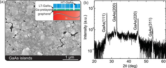
Figure 2: SEM plan-view image of a) 200nm high-temperature-grown GaAs on top of a 25nm-thick nucleation layer, with Ga pre-layer and b) x-ray diffraction scans for GaAs grown by two-step growth, showing polycrystallinity with the presence of GaAs (111), (200), (220), and (311).
Unfortunately, high temperatures are needed to crystallize GaAs and to suppress the effects of defects and dislocations through migration. The researchers suggest through theoretical considerations that the problem resides in low adsorption and migration energies of gallium and arsenic on multi-layer graphene that lead to cluster-growth at high temperature.
Based on their results, the researchers suggest that optimization of the growth parameters in terms of the pre-layer or the use of an alternative van der Waals material could lead to single-crystal 2D GaAs on Si. The team is also looking for a low-temperature or modified deposition technique that would eliminate the occurrence of 3D island growth at high growth temperatures.
GaAs on graphene/silicon substrate GaAs MBE Si substrate
http://dx.doi.org/10.1002/adfm.201400960
The author Mike Cooke is a freelance technology journalist who has worked in the semiconductor and advanced technology sectors since 1997.


