


- News
16 April 2015
Singapore's A*STAR develops one-step method for creating high-quality 2D materials
Shijie Wang at Singapore's A*STAR (Agency of Science, Technology and Research) Institute of Materials Research and Engineering (IMRE) and his collaborators have developed a technique for creating large areas of atom-thin two-dimensional (2D) semiconductor molybdenum disulfide for use in electronic devices (Tao J et al, 'Growth of wafer-scale MoS2 monolayer by magnetron sputtering', Nanoscale 7, 2497–2503 (2015)).
Molybdenum disulfide belongs to the transition-metal dichalcogenide (TMD) family of materials, which have two chalcogenide atoms (such as sulfur, selenium or tellurium) for every transition-metal atom (e.g. molybdenum and tungsten). These materials and their wide range of electrical properties provide an excellent platform material system for versatile electronics, but creating high-quality material over areas large enough for industrial-scale production is difficult.
"Traditional mechanical exfoliation methods for obtaining two-dimensional materials have limited usefulness in commercial applications, and all previous chemical methods are incompatible for integration with device fabrication," says Wang. "Our technique is a one-step process that can grow good-quality monolayer films, or few layers of molybdenum disulfide films, at wafer scale on various substrates using magnetron sputtering."
The team fired a beam of argon ions at a molybdenum target in a vacuum chamber, ejecting molybdenum atoms from the surface where they reacted with a nearby sulfur vapor. These atoms then assembled onto a heated substrate of either sapphire or silicon. The team found that they could grow monolayer, bilayer, trilayer or thicker samples by altering the power of the argon-ion beam or the deposition time.
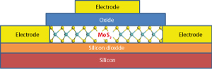 Graphic: Transistors made of films of 2D MoS2 could be integrated with other silicon electronics devices.
The quality of the material was confirmed using a number of common characterization tools including Raman spectroscopy, atomic force microscopy (AFM), x-ray photoelectron spectroscopy (XPS) and transmission electron microscopy (TEM). The electrical properties of the molybdenum disulfide films were also demonstrated by creating a working transistor.
"Our next step in this work will focus on the application of this technique to synthesize other two-dimensional materials and integrate them with different materials for various device applications," says Wang.
A*STAR Metal dichalcogenide heterostructure
www.imre.a-star.edu.sg/page.php?id=N534H532


