


- News
1 April 2015
Direct demonstration of 1THz performance in InP HEMTs
Northrop Grumman Corp in the USA is claiming the first ever direct demonstration of gain at 1THz in indium phosphide (InP) high-electron-mobility transistors (HEMTs) [X. B. Mei et al, IEEE Electron Device Letters, published online 24 February 2015]. Usually, claims of 1THz+ frequency performance are made on the basis of extrapolations from lower-frequency measurements. The team has also developed a 10-stage amplifier circuit based on the technology.
Northrop Grumman Aerospace Systems (NGAS) has been developing high-frequency transistor performance over two decades (Table 1). Researchers at NGAS have also been developing terahertz monolithic integrated circuit (TMIC) processing techniques to enable wiring together the transistors into amplifier circuits with gain beyond 1THz.
Table 1: Summary of InP HEMT processes developed at NGAS.
| Gate length | 100nm | 70nm | 35nm | 30nm | 25nm (latest work) |
| Year | 1998 | 2003 | 2007 | 2010 | 2013 |
| InxGa1-xAs channel indium composition | 60% | 75% | 100% | 100% | 100% |
| Source-drain spacing (μm) | 2 | 2 | 1.5 | 1.0 | 0.5 |
| Rc (Ω-mm) | 0.12 | 0.1 | 0.04 | 0.04 | 0.04 |
| gmp @ 1V (mS/mm) | 1000 | 1400 | 2000 | 2500 | 3000 |
| fMAX (THz) | 0.4 | 0.6 | 1.1 | 1.3 | 1.5 |
| Associated fT (THz) | 0.2 | 0.25 | 0.4 | 0.5 | 0.61 |
| Highest-frequency amplifier demonstrated (THz) | 0.19 | 0.24 | 0.48 | 0.85 | 1.0 |
| Associated amplifier device width (μm) | 30 | 30 | 20 | 14 | 8 |
The researchers write of their achievement of 1THz-capable HEMTs and the associated amplifier circuit: "The transistor and next-generation circuits will find applicability in a variety of emerging applications at THz frequencies, including high-data-rate communication systems, atmospheric sensing, planetary exploration, and new classes of imagers."
The researchers see "transistor gate and layout scaling for parasitic reduction, epi material enhancement for improved electron transport properties, and process improvement associated with the aggressive scaling" as being key technologies for their achievement.
The transistor heterostructures were grown on semi-insulating InP by molecular beam epitaxy (MBE). The 95Å composite channel was indium arsenide (InAs) sandwiched between two lattice-matched indium gallium arsenide (In0.53Ga0.47As) layers. The channel carrier concentration was enhanced with silicon-doping planes above and below the channel. The Hall mobility was 13,000cm2/V-s with 4x10¹²/cm2 carrier density. The barrier layer was 20Å thick, measured between the bottom of the gate and the upper silicon-doped plane.
The HEMTs were fabricated with unalloyed titanium/platinum/gold ohmic contacts. The source-drain distance was reduced to 0.5μm to give low source resistance of 130mΩ-mm and contact resistance of 40mΩ-mm. The recessed T-shaped gate of titanium/platinum/gold had a 25nm footprint. The device was also passivated with silicon nitride grown by chemical vapor deposition (CVD). The aim of the passivation was to improve reliability and robustness.
The TMIC wiring process capability includes nickel-chromium thin-film resistors, metal-insulator-metal capacitors and two levels of metal interconnect. The second metal level can be air-bridged to give higher signal speed over dielectric insulated wiring. The back-end processing also includes wafer thinning to 18μm and full metalized back-side vias.
Frequency performance measurements were carried out over three bands: 10GHz-110GHz, 500GHz-700GHz, and 750GHz-1.0THz. The available gain at 1.0THz was ~3.5dB. Extrapolating the data to unity gain gave a maximum oscillation frequency (fMAX) of 1.5THz. The cut-off frequency (fT) was 650GHz.
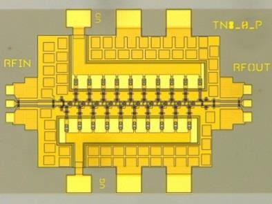 Figure 1: Microphotograph of 1.0THz TMIC amplifier.
The TMIC process was used to create a 10-stage 1.03THz common-source amplifier, based on 8μm wide HEMTs (two 4μm fingers). The circuit (Figure 1) also included matching, DC-blocking and decoupling capacitors. The TMIC is described as a 'first iteration' scaling of a previous 850GHz design. The researchers expect improvement and optimization from future iterations.
The frequency performance was measured on equipment capable of 750GHz-1100GHz testing. The circuit achieved 9dB gain at 1.0THz - "the first demonstration of transistor amplifier gain at or above the 1.0THz mark", according to the researchers (Figure 2). At 1.05THz the gain reduced slightly to 7dB.
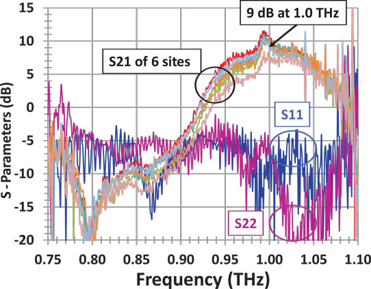
Figure 2: On-wafer measurement results showing 9dB on-wafer gain at 1.0THz.
The researchers comment: "This transistor and TMIC technology shows promise in enabling a new suite of components bridging microwave through THz frequencies." The 1THz shares "significant commonality" with NGAS' existing space-qualified 100nm InP HEMT technology, indicating a variety of space and airborne applications.
Northrop Grumman InP HEMTs InGaAs TMIC InP MBE
http://ieeexplore.ieee.org/xpl/articleDetails.jsp?arnumber=7047678
The author Mike Cooke is a freelance technology journalist who has worked in the semiconductor and advanced technology sectors since 1997.


