


- News
27 April 2015
Sidewall emission-enhancement for deep ultraviolet light-emitting diodes
Researchers in Korea and USA have developed sidewall emission-enhanced (SEE) deep ultraviolet (DUV) light-emitting diodes (LEDs) to improve light extraction efficiency [Dong Yeong Kim et al, Light: Science & Applications, vol4, e263, published online 10 April 2015].
DUV LEDs with wavelengths less than 300nm become very inefficient due to an increasing tendency for the photons to be emitted in the plane of the device. The problem arises from the band structure of high-aluminium-content aluminium gallium nitride (AlGaN) used for short-wavelength LEDs.
In such materials the dominant electron transition is from the conduction band to a crystal-field split-off hole state in the valence band. This transition emits photons with transverse magnetic polarization that propagates perpendicular to the c-direction of the crystal structure.
There has been some progress in improving DUV LEDs, with an external quantum efficiency (EQE) of 10% reported for 278nm wavelengths. However, commercial devices languish around 5% EQE. These values fall far short of the EQE of more than 80% for visible LEDs based on gallium indium nitride (GaInN).
If these problems can be overcome, applications beckon such as air/water/food purification/sterilization, polymer curing, semiconductor photolithography, and high-density optical recording. LEDs would then be able to replace bulky, fragile, poisonous mercury lamps or more complex, expensive systems.
The researchers from Pohang University of Science and Technology and Samsung Electronics in Korea and Rensselaer Polytechnic Institute in the USA have developed the SEE structure to enable better extraction of the in-plane transverse-magnetic radiation.
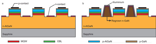
Figure 1: Device geometries. (a) Schematic of the conventional DUV LED structure (reference device) having narrow mesa stripes and (b) a proposed SEE DUV LED structure.
To enable extraction of light directed in the plane of the 1mmx1mm LED chip, multiple narrow mesa strips were formed through 1μm reactive ion etch into the wafer (Figure 1). Selective metal-organic vapor phase epitaxy (MOVPE) re-growth of n-GaN with silicon dioxide masking was used to create mirror structures in the gap between the strips.
The n-contacts of 900°C-annealed titanium/aluminium/nickel/gold were formed on these n-GaN trapezoid cross-section micro-structures, along with other n-AlGaN exposed regions. The p-contact was 650°C-anneal nickel/gold. The LED was completed with evaporation of aluminium to form a mirror surface on the n-GaN micro-structures and deposition of titanium/gold contact pads.
The DUV 285nm-wavelength emitting wafer (Figure 2) included a five-period Al0.4Ga0.6N/Al0.55Ga0.45N multiple quantum well grown on 4-inch c-plane sapphire by MOVPE.
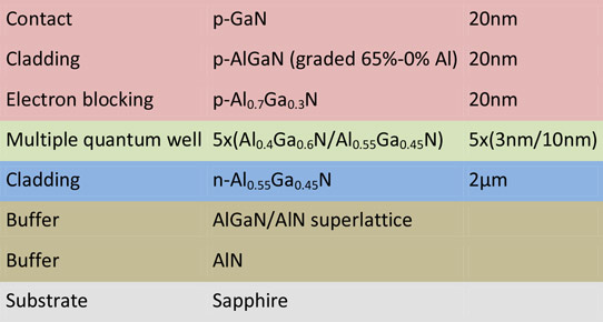
Figure 2: DUV LED wafer.
The stripes increase the effective perimeter of the device out of which light emerges, increasing light output power (LOP), EQE, and light extraction efficiency (LEE) (Figure 3). At the same time, the internal quantum efficiency (IQE) droops somewhat, due to an increase in current density in the reduced active region area for a given injection current. The placement of the n-GaN micro-structures in the gap between the mesa strips also increases output power.
The researchers explain: "Compared with reference LEDs with the same number of stripes, SEE DUV LEDs show higher LOPs because a part of the emitted DUV photons through the sidewalls is more likely to be reabsorbed by the MQW and the p-GaN contact formation layer of the neighboring mesa stripes in the reference LEDs than be reflected by the Al reflectors in the SEE DUV LEDs."
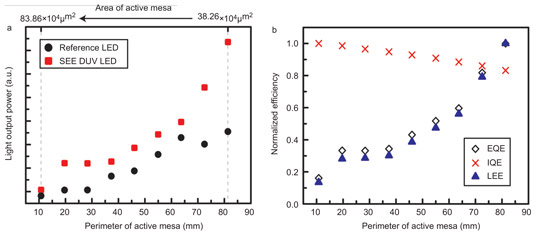
Figure 3: (a) LOPs of reference and SEE DUV LEDs measured in surface normal direction at injection current of 100mA as function of perimeter of active region. (b) Normalized EQE, IQE and LEE of SEE DUV LEDs.
The researchers also believe there is improved efficiency due to the shorter lateral distance that electrons have to travel from the n-contacts and the active regions of the devices when the strips are narrower, giving a larger perimeter.
Angular-dependent measurements showed strong emission from the sidewalls in the reference LEDs without n-GaN micro-structure mirrors. The SEE LEDs gave more radiation in the forward direction, similar to the pattern of c-plane GaInN LEDs.
SEE LEDs with 45 stripes also had a reduced forward voltage of 7.55V at 100mA compared with the reference devices, which needed about 0.25V larger bias for the same current. Both types of device showed reduced forward voltage requirements as the effective perimeter increased.
The improved forward voltage of the SEE LED was attributed to the better ohmic contact with the re-grown n-GaN and the larger contact area, compared with the contact with the flat n-AlGaN surface.
The researchers say there are various ways in which the mirror micro-structures can be changed by altering the process. A version for bottom emission through the substrate is being developed to take advantage of flip-chip devices that allow heat dissipation through a suitable sub-mount rather than thermally insulating sapphire.
The researchers point out that, as the aluminium content of the active region increases to access even shorter wavelengths, the SEE DUV LED structure will become even more effective, since a larger proportion of the emitted photons will be in the plane of the MQW.
www.nature.com/lsa/journal/v4/n4/abs/lsa201536a.html
The author Mike Cooke is a freelance technology journalist who has worked in the semiconductor and advanced technology sectors since 1997.


