


- News
16 April 2015
Current gain achieved in III-nitride hot-electron transistors
Researchers at University of California Santa Barbara (UCSB) have claimed current gain for the first time in III-nitride hot-electron transistors (HETs) using base current controlled common emitter characteristics [Geetak Gupta et al, IEEE Electron Device Letters, published online 25 March 2015].
HETs are vertical unipolar devices with an emitter that injects high-energy electrons across a base region, at the end of which transit the electrons are filtered and collected. The filtering of high-energy electrons is achieved with quantum barrier regions above and below the base.
The transport across the base region is ballistic – meaning that the mean free path is greater than the base thickness. This is in contrast to bipolar transistors that use diffusion effects in their operation. Potentially, HETs could operate with shorter delays and at higher frequency compared with bipolar transistors. To be useful, HETs require gain greater than 1, low base-collector leakage current, and low base resistance.
HETs are often produced using III-arsenide and/or III-antimonide materials. The combination of these semiconductor families allows the creation and use of large band discontinuities for the barriers. The III-nitride family contains a large range of band discontinuities that have recently been used to create HETs. However, these devices have been limited to current gains of the order of 0.1 (i.e. losses rather than gain) up to now.
The charge polarization of the III-nitride chemical bond was used to set up polarization dipole layers at various positions in the device to induce barriers (Figure 1). In particular, layers of aluminium nitride (AlN) and In0.1Ga0.9N were used to create emitter and collector barriers, respectively. The polarization properties of III-nitrides was also used to increase the conductivity of the base region by inducing a two-dimensional electron gas (2DEG). The 2DEG was also enhanced through modulation doping in the emitter.
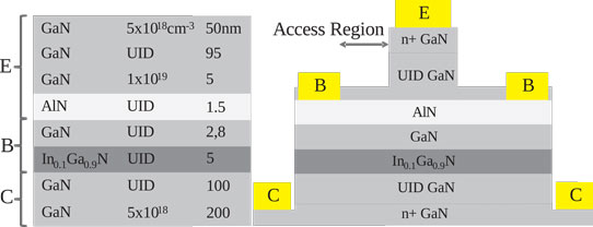
Figure 1: (a) Layer structure of as-grown III-N HETs for samples B1 and B2 (8nm and 2nm GaN, respectively) and (b) structure of fabricated device.
The structures were grown using plasma-assisted molecular beam epitaxy (PAMBE) on sapphire substrates. The GaN layer in the base region was either 8nm or 2nm.
The collector GaN layers were grown at 700°C. The temperature was then reduced to 570°C to grow the base-collector InGaN barrier. This was covered with 4nm or 1nm of low-temperature 570°C GaN, before raising the temperature to grow the rest of the device.
The low-temperature GaN layer was designed to protect the InGaN layer from decomposition in the subsequent growth. The need for the protection layer sets a lower limit on the base thickness (tB = GaN + InGaN = 8nm/2nm + 5nm).
The etching for the device fabrication used a combination of reactive-ion etching and inductively coupled plasma etching techniques. The AlN layer served as a stop layer for the inductively coupled plasma etch. A post-etch anneal was carried out at 400°C in nitrogen for 10 minutes. The base contact of aluminium/gold was then formed on the AlN, giving a tunnel junction access to the base region 2DEG. Further reactive-ion etching exposed the collector, before deposition of the ohmic emitter/collector contacts.
The thickness of the AlN layer had to be thick enough for the 2DEG to form, but also sufficiently thin to enable the base contact tunnel junction to remain ohmic. The researchers comment: "The multiple purposes served by the AlN layer enable us to aggressively scale the base thickness."
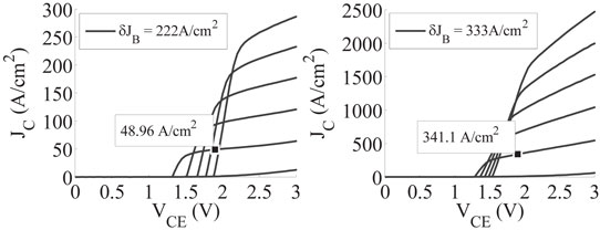
Figure 2: Common-emitter characteristics of HET structures (a) B1 and (b) B2. The collector current density (JC) curves correspond to six base current (JB) steps from 0 to 5δJB.
The base contact and sheet resistances of the sample B1 with 8nm GaN layer were 0.49Ω-mm and 1787Ω/square, respectively, lower than the values for sample B1 (2nm GaN, 1.44Ω-mm, 3550Ω/square). The mobility degradation for B1 is attributed to alloy scattering in the underlying InGaN layer.
Common-emitter measurements gave a current gain of 0.22 for B1 and 1.02 for B2. The researchers comment: "Since the only difference between the two samples is the GaN thickness, the increase in gain can be directly attributed to the decrease in tB from 13nm to 7nm." The reverse bias base-collector leakage for both B1 and B2 was ~100A/cm2.
The researchers believe that further progress to higher gain needs thinner bases, while maintaining low base contact and sheet resistances. Better understanding of the quantum mechanical reflections at the base-collector barrier should also lead to better performance.
III-nitride hot-electron transistors GaN AlN InGaN PAMBE Sapphire substrates
http://ieeexplore.ieee.org/xpl/login.jsp?tp=&arnumber=7067388
The author Mike Cooke is a freelance technology journalist who has worked in the semiconductor and advanced technology sectors since 1997.


