


- News
17 August 2015
Berkeley Lab' Campanile probe reveals nanoscale optoelectronic heterogeneity within monolayer MoS2 accompanied by 300nm-wide, energetically disordered edge region
The US Department of Energy (DOE)'s Lawrence Berkeley National Laboratory (Berkeley Lab) has used its unique 'Campanile' nano-optical probe in the Molecular Foundry (a DOE Office of Science User Facility) to study the effects of illumination - at the molecular level - on two-dimensional semiconductors, specifically MoS2, a member of the transition metal dichalcogenide (TMDC) family of semiconductors, whose optoelectronic properties hold great promise for future nanoelectronic and photonic devices ('Visualizing nanoscale excitonic relaxation properties of disordered edges and grain boundaries in monolayer molybdenum disulfide', Nature Communications, 6, no 7993, doi:10.1038/ncomms8993).
"The Campanile probe's remarkable resolution enabled us to identify significant nanoscale optoelectronic heterogeneity in the interior regions of monolayer crystals of molybdenum disulfide, and an unexpected, about 300nm-wide, energetically disordered edge region," says James Schuck, a staff scientist in Berkeley Lab's Materials Sciences Division who led the study as well as the team that created the Campanile probe (which combines the advantages of scan/probe microscopy and optical spectroscopy).
"This disordered edge region, which has never been seen before, could be extremely important for any devices in which one wants to make electrical contacts," Schuck says. "It might also prove critical to photocatalytic and nonlinear optical conversion applications." Schuck, who directs the Imaging and Manipulation of Nanostructures Facility at the Molecular Foundry, is the corresponding author of the paper. Co-lead authors are Wei Bao and Nicholas Borys.
2D-TMDCs rival graphene as potential successors to silicon for the next generation of high-speed electronics. Single-molecule-thick 2D-TMDC materials have superior energy efficiencies and a capacity to carry much higher current densities than silicon. However, since their experimental discovery in 2010, their performance has lagged far behind theoretical expectations, primarily because of a lack of understanding of 2D-TMDC properties at the nanoscale, particularly regarding excitons (bound pairs of excited electrons and holes that enable semiconductors to function in devices).
"The poor understanding of 2D-TMDC excitonic and other properties at the nanoscale is rooted in large part to the existing constraints on nanospectroscopic imaging," Schuck says. "With our Campanile probe, we overcome nearly all previous limitations of near-field microscopy and are able to map critical chemical and optical properties and processes at their native length scales," he claims.
The Campanile probe (named after the landmark 'Campanile' clock tower on the University of California at Berkeley campus) features a tapered, four-sided microscopic tip that is mounted on the end of an optical fiber. Two of the probe's sides are coated with gold and the two gold layers are separated by just a few nanometers at the tip. The tapered design enables the probe to channel light of all wavelengths down into an enhanced field at the apex of the tip. The size of the gap between the gold layers determines the resolution, which can be below the diffraction optical limit.
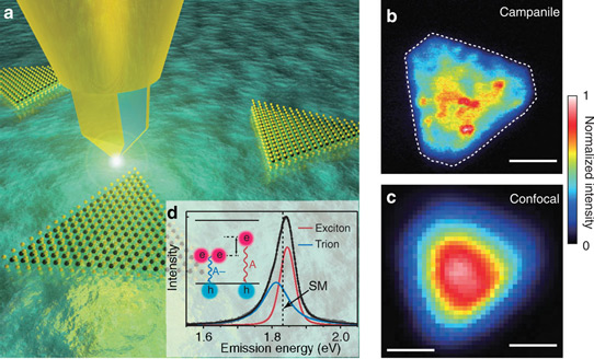
(a) Near-field excitation and collection of photoluminescence from monolayer (ML)-MoS2 using Campanile probe where the optical laser excitation (2.33 eV) and collection of sample emission are confined to tip apex to produce high-resolution optical maps. (b) Map of PL emission intensity of a triangular ML-MoS2 flake using Campanile probe. White dashed line indicates flake boundary as determined from the shear-force topography. (c) Image acquired with scanning confocal microscopy using x100, 0.7NA air objective. Scale bars, 1 μm. (d) Near-field nano-PL spectrum averaged over spatial extent of the ML-MoS2 flake.
The researchers used the Campanile probe to spectroscopically map nanoscale excited-state/relaxation processes in monolayer crystals of molybdenum disulfide that were grown by chemical vapor deposition (CVD). MoS2 is a 2D semiconductor that features high electrical conductance comparable to that of graphene but, unlike graphene, has natural energy bandgaps (so its conductance can be switched off).
"Our study revealed significant nanoscale optoelectronic heterogeneity and allowed us to quantify exciton-quenching phenomena at crystal grain boundaries," Schuck says. "The discovery of the disordered edge region constitutes a paradigm shift from the idea that only a 1D metallic edge state is responsible for all the edge-related physics and photochemistry being observed in 2D-TMDCs," he adds. "What's happening at the edges of 2D-TMDC crystals is clearly more complicated than that. There's a mesoscopic disordered region that likely dominates most transport, nonlinear optical, and photocatalytic behavior near the edges of CVD-grown 2D-TMDCs."
The researchers also discovered that the disordered edge region in MoS2 crystals harbors a sulfur deficiency that has implications for future optoelectronic applications of this 2D-TMDC. "Less sulfur means more free electrons are present in that edge region, which could lead to enhanced non-radiative recombination," Schuck says. "Excitons created near a sulfur vacancy would live for a much shorter period of time."
The researchers plan to next study the excitonic and electronic properties that may arise, as well as the creation of p-n junctions and quantum wells, when two disparate types of TMDCs are connected.
"We are also combining 2D-TMDC materials with so-called meta surfaces for controlling and manipulating the valley states and circular emitters that exist within these systems, as well as exploring localized quantum states that could act as near-ideal single-photon emitters and quantum-entangled Qubit states," Schuck concludes.
Metal dichalcogenide heterostructure Molybdenum disulfide
www.nature.com/ncomms/2015/150813/ncomms8993/full/ncomms8993.html
http://foundry.lbl.gov/schuckgroup


