


- News
26 August 2015
Microwave anneal process for gallium nitride transistors
Fudan University in China claims the first reported application of microwave annealing (MWA) to the formation of ohmic source-drain contacts to aluminium gallium nitride/gallium nitride (AlGaN/GaN) high-electron-mobility transistors (HEMTs) [Lin-Qing Zhang et al, IEEE Electron Device Letters, published online 28 July 2015]. The MWA process improved on/off current ratios, lower gate leakage, and maximum drain current, compared with devices fabricated using rapid thermal annealing (RTA).
GaN HEMTs are being developed for high-power, high-voltage and high-frequency applications.
The device structure consisted of a silicon substrate, 2.5μm carbon-doped GaN buffer, 500nm intrinsic GaN channel, 1nm AlN interlayer, 23nm undoped Al0.25Ga0.75N barrier, and 5nm GaN cap. Fabrication began with mesa isolation plasma etch.
The titanium/aluminium/nickel/gold ohmic contact stack was deposited using evaporation and patterned using lift-off lithography. The 5.8GHz MWA was carried out using 4200W power for 20 minutes in nitrogen. A comparison device was also produced using rapid thermal annealing (RTA) at 840°C for 30 seconds in nitrogen.
The Ohmic contact resistance, derived from transmission-line method structures, was 0.4Ω-mm for RTA and 0.6Ω-mm for MWA. Before annealing, Hall measurements gave a channel sheet resistance of 435Ω/square. For RTA, this was increased to 474Ω/square. The MWA process had a smaller increase to 464Ω/square.
Microscopic inspection of the contacts showed a dark bumpy surface for the RTA process, as opposed to a smoother brighter appearance under MWA. The researchers attribute the difference to the lower process temperature of 597.6°C for MWA. Atomic force microscopy (AFM) over a 10μmx10μm area gave a root-mean-square roughness of 63.5nm for MWA contacts and 101nm for RTA.
While RTA heats the surface region, MWA penetrates more deeply into the structure, allowing lower peak temperatures to achieve its effect. High-resolution transmission electron microscopy (HR-TEM) suggests that contact with the GaN channel layer is made through titanium nitride spike protrusions that form along dislocations (Figure 1).
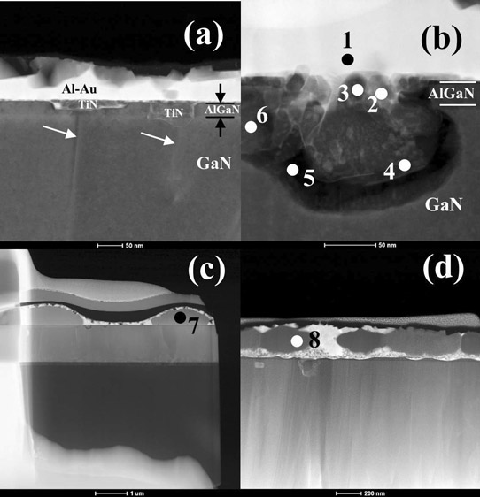
Figure 1: (a) TEM image of post-annealing structure by MWA where arrow markings indicate dislocations. (b) Magnified image of interface. (c) TEM image of bulge area of alloyed ohmic contact treated by RTA. (d) TEM image of bulge area of alloyed ohmic contact treated by MWA.
The transistors were completed with a T-shaped nickel/gold gate. The footprint was 100nm with 60μm gate width. One effect of using MWA is to decrease off-current leakage, improving the on/off current ratio to 4x10⁴ at 10V drain bias (Figure 2). The on-current was measured at +2V gate potential and the off-current at -2.5V.
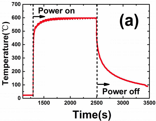
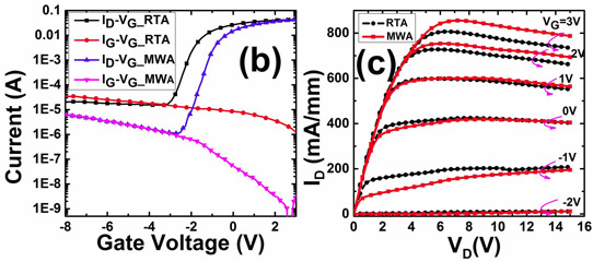
Figure 2: (a) Temperature profile of MWA process at 4200W power. (b) Comparison of transfer characteristics of samples treated by MWA and RTA. (c) Output characteristics of samples treated by RTA and MWA.
The source of off-current leakage was mainly through the gate. The researchers comment: "It is shown that the gate leakage current of MWA-HEMT is significantly lower than that of RTA-HEMT. The suspected cause is that MWA has better ability in repairing defects of AlGaN surface."
The MWA device also had a larger maximum drain current of 850mA/mm, compared with 800mA/mm for RTA.
http://ieeexplore.ieee.org/xpl/articleDetails.jsp?arnumber=7169554
The author Mike Cooke is a freelance technology journalist who has worked in the semiconductor and advanced technology sectors since 1997.


