


- News
28 August 2015
High-performance gallium nitride on low-resistance silicon
University of Glasgow and University of Cambridge in the UK have claimed the highest frequency performance to date for gallium nitride (GaN) high-electron-mobility transistors (HEMTs) on low-resistivity (LR) silicon (Si) [A. Eblabla et al, IEEE Electron Device Letters, published 23 July 2015]. The researchers see the technology as making viable cost-effective X-band and higher-frequency applications. In addition, the team sees potential for such GaN devices in mobile communications where power management and radio frequency (RF) functions could be integrated on silicon.
Normally, high-resistivity (HR) substrates are preferred for high-frequency devices to avoid losses from coupling with RF signals. However, even high resistance silicon is expensive.
The devices (Figure 1) were grown on 150mm silicon substrates with resistivity less than 10Ω-cm, using metal-organic chemical vapor deposition (MOCVD). The 850nm iron-doped aluminium gallium nitride (AlGaN) buffer was graded to accommodate lattice and thermal expansion mismatch between GaN and silicon. The 1.4μm GaN buffer was also iron-doped, giving it an insulating character.
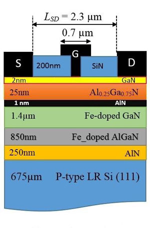 Figure 1: Cross-sectional schematic view of fabricated T-gate AlGaN/AlN/GaN epilayer grown on LR p-type Si (111) substrate with Si3N4 passivation.
The researchers report: "The wafer was completely crack free with wafer bow after cooling from the growth temperature (1050°C) of 22μm (concave). This demonstrates that the lattice and thermal mismatch strains are well managed in the buffer layers and the wafer bow is compatible with processing through a commercial silicon fab."
Hall measurements on the two-dimensional electron gas (2DEG) in the GaN channel region gave 8.1x10¹²/cm2 carrier density, 1700cm2/V-s mobility and 412Ω/square sheet resistance.
The transistor was fabricated using electron-beam lithography. The ohmic source-drain contacts consisted of titanium/aluminium/molybdenum/gold alloy. Following mesa isolation, silicon nitride was deposited as passivation and then nickel-chromium/gold for the T-gate.
The maximum saturation current was 1.4A/mm at 10V drain and +1V gate for a device with 0.3μm gate length and 2x100μm width. The pinch-off at -4V is described as 'well-behaved'. The on-resistance was 2.76Ω-mm. The maximum transconductance of 425mS/mm was achieved at 5V drain and -3.2V gate bias. The leakage current was 18.5nA/mm for 10V drain and -3.5V gate.
The researchers comment: "The excellent performance of these GaN-on-LR Si devices is the result of a well-engineered material growth, device layout and fabrication process quality in addition to proper passivation techniques. Moreover, these excellent results are competitive with other reported GaN HEMTs on high-resistivity substrates including sapphire and HR Si substrates."
For frequency measurements, the small-signal gain was maximized by the bias point of 5V drain and -3.2V gate. The maximum current gain frequency (fT) was 55GHz and the maximum oscillation frequency (fmax) was 121GHz, correcting ('de-embedding') for parasitic pad capacitances and inductances.
"To our knowledge these are the best RF performance of GaN-based HEMTs on LR Si to date," the researchers write. They also point out that their RF results exceed in certain respects reports of devices on sapphire and high-resistivity silicon. For example, the fT of GaN HEMTs on high-resistivity silicon have reached 54GHz, while fmax was 184GHz.
The researchers believe that improved performance could be achieved with shorter gate lengths, thinner Al0.25Ga0.75N top-barrier, thicker GaN buffer and lower-resistance ohmic contacts.
http://ieeexplore.ieee.org/xpl/articleDetails.jsp?arnumber=7165603
The author Mike Cooke is a freelance technology journalist who has worked in the semiconductor and advanced technology sectors since 1997.


