


- News
5 August 2015
Tellurium doping for n-type indium gallium arsenide
Researchers in the USA claim a record active doping concentration of 8x10¹⁹/cm3 for n-type indium gallium arsenide (In0.53Ga0.47As) grown on 300mm silicon (Si) wafers by metal-organic chemical vapor deposition (MOCVD) using diethyl-telluride (DETe) as the dopant source [Tommaso Orzali et al, Journal of Crystal Growth, vol426, p243, 2015]. The work involved SEMATECH, Aixtron Inc, and State University of New York (SUNY) Polytechnic Institute.
The team sees potential application in re-grown source-drain (S/D) structures for future InGaAs high-mobility-channel transistor very large scale integration (VLSI) electronics. Silicon is the most common dopant for n-InGaAs. Unfortunately, as a group IV element it is amphoteric, meaning that it can act as a donor or acceptor. Silicon begins to auto-compensate at 5x10¹⁸/cm3 electron concentration, limiting free carriers to around 1019/cm3.
The researchers used an Aixtron CRIUS-R 300mm system to perform MOCVD of In0.53Ga0.47As on 3-inch indium phosphide (InP) and 300mm Si (100) substrates. The precursors were trimethyl-gallium, trimethyl-indium, arsine, and diethyl-telluride in palldium-purified hydrogen carrier. The attractive properties of diethyl-telluride for MOCVD include being a liquid up to 136°C, low reactivity with air or water, and a vapor pressure of 12Torr at 30°C.
Table 1: Hall and SIMS data for Te-doped In0.53Ga0.47As on 3-inch InP wafers grown at 660°C.
| DETe (μmol/min) | V/III ratio | Sheet resistance (Ω/square) | Mobility (cm2/V-s) | Active electron density (1019/cm3) | Tellurium concentration (1019/cm3) | Activation efficiency (%) |
| 0.024 | 44 | 13.6 | 1310 | 3.5 | 5.8 | 60.3 |
| 0.13 | 44 | 43.5 | 1100 | 1.3 | 6.6 | 19.6 |
| 0.13 | 22 | 13.8 | 1320 | 3.4 | 5.7 | 59.6 |
| 1.2 | 44 | 24.4 | 1110 | 2.3 | 10 | 23 |
On InP, active electron densities higher than 1x10¹⁹/cm3 were easily achieved at a growth temperature of 660°C and a V/III ratio of 44 (Table 1). This level was produced by diethyl-telluride flows as low as 0.024μmol/min, giving a dopant concentration of 5.8x10¹⁹/cm3 and an active electron density of 3.5x10¹⁹/cm3 (efficiency 60.3%). Increasing the flow by 50x only increased the dopant level to 10x1019/cm3, but since the activation efficiency was then only 23%, the active electron density was reduced to 2.3x10¹⁹/cm3.
The volatile nature of tellurium leads to a surfactant behavior and segregation at step edges of the growing InGaAs crystal structure. At higher growth temperature the tellurium tends to evaporate rather than be incorporated into the crystal.
Reducing the V/III ratio to 22 to ease the substitution of tellurium for arsenic in the InGaAs structure with 0.13μmol/min diethyl-telluride flow increased the activation efficiency from 19.6% to 59.6%. The respective dopant concentrations were 6.6x10¹⁹/cm3 and 5.7x10¹⁹/cm3. The active electron densities were 1.3x10¹⁹/cm3 and 3.4x10¹⁹/cm3, respectively.
The active electron density therefore seems to saturate around 3.5x10¹⁹/cm3 for growth at 660°C.
For growth on 300mm silicon, the process was used on an InP/GaAs buffer that bridged the 8% In0.53Ga0.47As/Si lattice mismatch. A highly resistive 300nm indium aluminium arsenide barrier was inserted between the buffer and InGaAs to ensure electrical isolation from the buffer. The InGaAs/InAlAs/InP were lattice matched. The bandgap of the InAlAs was 1.47eV, confining the electrons to the InGaAgs layer (~0.75eV).
Table 2: Hall and SIMS data for Te-doped In0.53Ga0.47As as function of growth temperature.
| Temp(°C) | Substrate | Sheet resistance (Ω/square) | Mobility (cm2/V-s) | Active electron density (1019/cm3) | Activation efficiency (%) |
| 500 | Si | 12.1 | 841 | 8.0 | 14.5 |
| 600 | Si | 44.2 | 970 | 4.4 | 62.8 |
| 660 | InP | 13.8 | 1320 | 3.4 | 59.6 |
Attempting to improve tellurium incorporation, the researchers varied the growth temperature down to 500°C for the InGaAs growth with 22 V/III ratio and 0.13μmol/min diethyl-telluride flow (Table 2). At 500°C, the active electron density was 8x10¹⁹/cm3, with 14.5% activation efficiency on a 5.5x10²⁰/cm3 tellurium concentration.
The researchers comment: "a carrier concentration of 8x10¹⁹/cm3 is, to the best of our knowledge, amongst the highest values reported for MOCVD grown In0.53Ga0.47As [see Figure 1]."
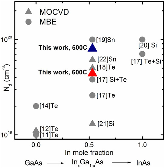
Figure 1: InxGa1-xAs active carrier concentration benchmarking.
The sheet resistance of a 100nm tellurium-doped InGaAs layer grown at 500°C was 9.53Ω/square with 0.8% coefficient of variation (standard deviation/mean). "This is an excellent value considering that the layer is grown at 500°C, in the MOCVD kinetic controlled regime, where a slight temperature non-uniformity can severely affect the alloy composition and the dopant concentration," the researchers write.
The surfactant properties of tellurium on InGaAs growth at 600°C reduced root-mean-square surface roughness from 3.6nm for undoped material to 0.4nm for heavily Te-doped InGaAs in 5μmx5μm atomic force microscopy (AFM) scans. At 500°C, the surface roughness of Te-doped InGaAs was 2.3nm.
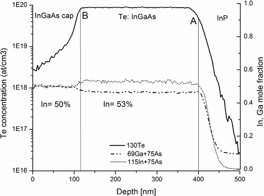
Figure 2: SIMS profile of 300nmTe-doped InGaAs grown on InP/GaAs buffer heterostructure on Si capped with 110nm undoped InGaAs.
One drawback of the surfactant property of Te was the slow turn-off of doping when the researchers tried to create a 110nm undoped InGaAs cap on a 300nm Te-doped InGaAs layer, as revealed by secondary-ion mass spectroscopy (SIMS) – see Figure 2. The 'memory effect' is attributed to accumulation of Te on the growth surface retarding incorporation in the bulk material. At the surface of the cap layer, the Te concentration was ~1018/cm3.
The researchers comment: "Although the slow Te turn-off may not be important for the targeted VLSI S/D re-growth application, the slow turn-on will prevent the formation of an abrupt junction in the source/drain region, which is crucial for short-channel devices."
Possible ways to combat the memory effect include pulsing the dopant precursor before growth for sharp turn-on or inserting a post-growth bake after the doped layer to sublimate tellurium precursor products from the wafer surface.
The tellurium content also affected the indium composition of the InGaAs – the presence of higher concentrations of tellurium improves indium incorporation (and vice versa). Further, the tellurium atom is larger than arsenic, introducing compressive strain into the doped InGaAs. Care must be taken to avoid introducing dislocations from strain relaxation.
InGaAs Diethyl-telluride MOCVD SEMATECH Aixtron SUNY
www.sciencedirect.com/science/article/pii/S0022024815003541
The author Mike Cooke is a freelance technology journalist who has worked in the semiconductor and advanced technology sectors since 1997.


