


- News
13 August 2015
Improving aluminium nitride barriers with low-temperature pulsed MOCVD
Xidian University in China has applied pulsed metal-organic chemical vapor deposition (PMOCVD) to improve the quality of aluminium nitride (AlN) barrier layers on gallium nitride (GaN), compared with traditional MOCVD [JunShuai Xue et al, Appl. Phys. Lett., vol107, p043503, 2015]. Although better-quality AlN barriers can be achieved with molecular beam epitaxy (MBE), MOCVD is preferred for manufacturing.
The hope is to increase the carrier density in the two-dimensional electron gas (2DEG) that forms at the interface of AlGaN/GaN structures from the order of 1013/cm2 to ultimately around 6.4x10¹³/cm2 for AlN/GaN.
Such 2DEG regions lie at the heart of most nitride semiconductor transistors being developed for high-voltage, high-power and high-frequency electronics with potential application in power conversion and mobile communication network amplifiers.
The 2DEG forms as a result of the difference in spontaneous and strain-dependent charge polarization between the barrier and underlying GaN. AlN has the largest such difference with GaN. But these materials also have a large 2.4% lattice mismatch, which severely limits the thickness and quality of AlN barriers. In some cases, physical cracks become apparent.
The MBE process produces better-quality AlN barriers because it uses a much lower growth temperature than MOCVD. Lower temperature avoids effects from the decomposition of the GaN channel layer, such as roughening of the interface, which impacts the performance of the 2DEG.
Pulsed MOCVD allows the growth temperature of MOCVD to be lowered as a result of enhanced migration of growth precursors. The technique has been applied to indium aluminium nitride (InAlN) growth, resulting in high-performance high-electron-mobility transistors (HEMTs).
The researchers used a homemade close-coupled showerhead MOCVD reactor with quartz chamber and silicon-carbide-coated susceptor. The substrate was 2-inch c-plane sapphire. The group III metal precursors were trimethyl- organics. The nitrogen source was ammonia.
The growth was initiated with annealing and nitridation of the sapphire substrate at 1060°C. The nitride semiconductor layers (Figure 1) consisted of 620°C 20nm AlN, 1075°C 60nm AlN, 940°C 1.4μm GaN, and 830°C 4nm AlN barrier. All the layers, except for the barrier, were created using MOCVD in hydrogen.
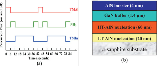
Figure 1: (a) Schematic diagram of PMOCVD pulse sequence for growth of AlN barrier and (b) schematic cross-section of AlN/GaN heterostructure.
The ambient gas for the PMOCVD barrier growth was changed to nitrogen. Also, indium was used as surfactant during the PMOCVD to improve adatom migration and improve surface quality. Atomic force microscopy (AFM) gave a root-mean-square roughness of 0.15nm, compared with 0.24nm from 4nm AlN grown by plain MOCVD at 830°C.
PMOCVD has been used to grow InAlN – by increasing the growth temperature, the indium incorporation is decreased. At 830°C, the indium incorporation is negligible, giving a quasi-binary AlN. This was confirmed by x-ray diffraction (XRD) and x-ray photoelectron spectroscopy (XPS) – see Table 1.
Table 1: XPS results for AlN/GaN heterostructure with 4nm AlN barrier, giving atomic percentage (%) of various species.
| Al | Ga | In | N | C | O |
| 33.44 | 2.84 | 0.24 | 35.52 | 12.50 | 15.46 |
The presence of oxygen and carbon is attributed to residue from the metal-organic precursors, native oxide, solvent treatment, etc. The gallium incorporation is most likely due to residue on the hot reactor walls from the previous processes, according to the researchers.
Also, the temperature is higher than for MBE so, while the unintentional gallium is reduced compared with higher-temperature MOCVD processes, it is not entirely removed, as in MBE-grown AlN.
The 2DEG at the AlN barrier interface with the GaN had, at room temperature, 1398cm2/V-s mobility and 1.3x10¹³/cm2 carrier density, giving a 344Ω/square sheet resistance (Figure 2). These values are comparable with results from AlGaN/GaN MOCVD heterostructures and an improvement on previous AlN/GaN material produced by MOCVD.
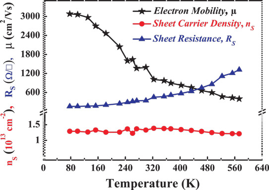
Figure 2: Temperature-dependent electron transport properties of AlN/GaN heterostructures with 4nm AlN barrier grown by PMOCVD.
The researchers comment: "This improvement is attributed to the enhanced quality of AlN barrier and heterointerface due to effectively avoiding etch and decomposition of underlying GaN channel in PMOCVD process under low growth temperature. So, the interface roughness scattering is remarkably reduced, thus leading to a considerably improved electron mobility. Further increase of carrier density would be expected by surface treatment such as deposition of SiN or oxide passivation layer on the AlN barrier surface."
HEMT devices were produced with titanium/aluminium/nickel/gold source–drain electrodes and a nickel/gold/nickel Schottky gate. The gate length was 0.6μm and the width was 2x50μm (i.e. 100μm total). The gate–drain separation was 2.5μm. The gate–source spacing was 0.9μm. There was no silicon nitride passivation.
The maximum drain current was 305mA/mm. The peak extrinsic transconductance of 95mS/mm was achieved at 10V drain bias and 1.8V gate potential. The researchers believe these values could be improved with better ohmic contact for the source-drain electrodes and the adoption of more advanced fabrication, such as electron-beam lithography.
AlN barrier layers MOCVD GaN HEMTs MBE
http://dx.doi.org/10.1063/1.4927743
The author Mike Cooke is a freelance technology journalist who has worked in the semiconductor and advanced technology sectors since 1997.


