


- News
18 December 2015
imec integrates indium gallium arsenide into vertical NAND memory structure
The imec research center in Belgium has integrated high-mobility indium gallium arsenide (InGaAs) channels into three-dimensional (3D) vertical NAND charge-trap flash memory structures. The research was reported at the International Electron Device Meeting in Washington DC, USA [IEDM session 3.1, 7 December 2014].
Silicon-based vertical 3D NAND flash memory has been in mass production at Samsung since 2013 (Figure 1). This year, Samsung moved from a 2-bit to a 3-bit architecture. Such devices are applied in Samsung's solid-state drives (SSDs). Key partners in the imec research were Samsung, Micron-Intel, Toshiba-Sandisk, SK Hynix, TSMC, and GlobalFoundries.
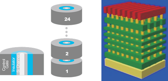
Figure 1: Samsung vertical NAND cells (left) and Toshiba vertical NAND stacking (right).
The NAND memory devices were formed in plugs/holes with diameters as small as 45nm. InGaAs channels improve transconductance and read current, enabling vertical NAND cost reduction by adding more layers in a stacked 3D architecture.
Planar NAND flash suffers from severe cell-to-cell interference and read noise due to aggressively scaled dimensions, reducing current levels. Present-day 3D NAND devices use polysilicon (poly-Si) channels where conductivity is affected by grain size distribution. Electrons are scattered at grain boundaries and charged defects, reducing current flow [imec also reported on modeling the impacts of such factors on poly-Si vertical NAND in session 5.6].
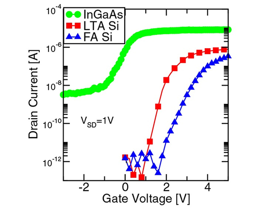
Figure 2: Drain current performance of imec InGaAs-channel vertical NAND element.
imec's InGaAs vertical NAND was created through a gate-first, channel-last process. The InGaAs channel was grown by metal-organic vapor phase epitaxy (MOVPE). imec says that the process demonstrated good III-V growth selectivity to silicon, allowing holes to be filled down to 45nm diameter. According to imec, the III-V channels outperformed poly-Si in terms of on-state current and transconductance (Figure 2), without degrading memory characteristics such as programming, erase and endurance.
An Steegen, senior vice president Process Technology at imec, comments: "While these results are shown on full channels, they are an important stepping stone to develop industry-compatible macaroni-type III-V channels."
The author Mike Cooke is a freelance technology journalist who has worked in the semiconductor and advanced technology sectors since 1997.


