


- News
1 December 2015
Thinning buffer layers for GaN-on-silicon light-emitting diodes
Plessey Semiconductors Ltd in the UK has been improving its indium gallium nitride (InGaN)-on-silicon light-emitting diode (LED) technology [Liyang Zhang et al, Journal of the Electron Devices Society, vol3, p457, 2015]. A light output power (LOP) of 563mW at 350mA injection was achieved. The wall-plug efficiency was 52.7%.
The researchers comment: "To the best of our knowledge, these results represent the first general lighting class high-brightness GaN-on-Si LEDs using thin buffer layer technology. The technology enables faster epitaxy process throughput and reduced manufacturing costs, while the manufacturability results attest its feasibility as a potential replacement of incumbent sapphire technology."
Further, the use of GaN-on-Si technology could also allow integration of bipolar transistors, Zener diodes and silicon photodiodes.
The team managed to reduce the epitaxial layer thickness to 3.75μm, where normally GaN-on-Si epilayers are between 6μm and 8μm.
Although production on silicon substrates promises reduced material and processing costs from the larger-diameter wafers (estimated 40-60% savings at die level), producing crack-free epilayers is challenging. The lattice constant mismatch is -17%. GaN and silicon also have different thermal expansion rates, with a +115% mismatch giving tensile stress on cool-down. By contrast, GaN buffers grown on sapphire have a smaller -34% mismatch, giving compression of the epilayer on cooling, which also has the advantage of tending to inhibit cracking.
The researchers report: "Device processing is performed in a wafer fab which used to be a depreciated CMOS manufacturing line. This facility allows the use of systems such as cassette-to-cassette wafer handling and semi-automated stepper lithography, which greatly improves process throughput."
Full implementation of automated processing equipment such as lithography stepper tools requires wafer bow to be controlled.
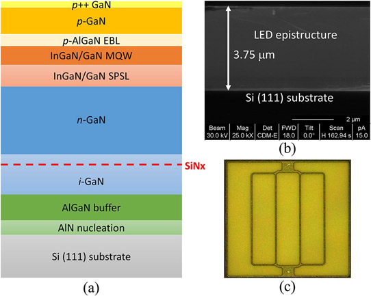
Figure 1: (a) Schematic diagram of LED epi-structure, (b) Scanning electron microscope (SEM) cross section and (c) device layout.
The LED epitaxial material (Figure 1) was grown on 150mm silicon (111) wafers using ~1000°C metal-organic chemical vapor deposition (MOCVD). The substrate was 1mm thick.
The aluminium nitride (AlN) nucleation and graded aluminium gallium nitride (AlGaN) buffer layers were 200nm and 600nm, respectively. The unintentionally doped gallium nitride (i-GaN) buffer consisted of a slow-growth 800nm layer for recovery of crystallinity from the highly defective AlGaN, and silicon nitride interlayer for subsequent overgrowth of a thin layer of i-GaN. This was followed by 1.8μm of heavily silicon-doped n-GaN.
The LED active layer consisted of a 20-pair InGaN/GaN short-period superlattice (SPSL) and a 4-pair InGaN/GaN multiple quantum well (MQW). The p-type layers included an electron-blocking layer (EBL). Using a nitrogen atmosphere during the EBL growth improved incorporation of the magnesium dopant.
Atomic force microscope (AFM) analysis gave a dislocation density of 5x10⁸/cm2 on optimized structures. V-pits of ~100nm diameter formed on the dislocations above the superlattice layer with a 3.3x10⁸/cm2 density. Introducing a partial hydrogen ambient environment during growth of the GaN layers in the SPSL and MQW was found to reduce V-pit density and diameter. Wafer bow was reduced to less than 10μm.
The p-electrode consisted of a thin nickel contact and silver-based mirror. The titanium/aluminium n-contact was made to the Ga-face of the n-GaN layer. The researchers add: "To improve current spreading, an additional thicker Ti/Al electrode is formed directly above the n-electrode and is connected together through a series of small vias."
The wafer was then bonded to a silicon handle wafer to allow the growth substrate to be removed using chemical mechanical polishing (CMP) and wet etch. The AlN and AlGaN layers were removed with plasma etching. Potassium hydroxide was used to roughen the exposed n-GaN surface, improving light extraction.
The LED wafer was finally singulated into thin-film 1mmx1mm chips and mounted in 3.5mmx3.5mm plastic packages (3535).
The light output power (LOP) of bare dies was 480mW at 350mA injection and 3.05V forward potential (Figure 2). The dominant wavelength was 452nm. Encapsulated with a silicone domed lens allowed the LOP to be increased to 563mW, representing a wall-plug efficiency of 52.7% at 35A/cm2. Reducing the injection current density to 10A/cm2 would increase the efficiency to 64%.
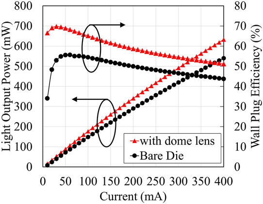
Figure 2: Light output power and wall-plug efficiency of bare die and dome lens packaged die as function of injection current.
The researchers quote, as state-of-the-art comparison, devices from Osram, produced on sapphire with similar configuration, that achieve 600-630mW LOP.
The hot-cold factor – the ratio of performance at 90°C/20°C – was 0.94. This is comparable with tier-1 devices on sapphire, according to the researchers.
Electroluminescence wavelength standard deviation over devices from 300 wafers was 2nm with a mean wavelength of 455nm. The researchers comment: "Statistically, this translates to 80% and 95% of the dies within a 5nm and 8nm bin range, respectively. This is a significant result, as LED die binning and sorting is a major cost and throughput overhead, and this technology paves the way for reduced binning and improved manufacturing yield."
Improved device reliability was indicated by 95% of devices having a 5V reverse-bias leakage less than 0.1μA.
GaN-on-silicon LEDs LEDs Plessey MOCVD
http://ieeexplore.ieee.org/xpl/articleDetails.jsp?arnumber=7174951
The author Mike Cooke is a freelance technology journalist who has worked in the semiconductor and advanced technology sectors since 1997.


