


- News
26 February 2015
Stressed out InAlN/GaN fin-HEMT boosts performance
Researchers based in Singapore and USA have stress engineered three-dimensional (3D) triple T-gate (TT-gate) lattice-matched indium aluminium nitride/gallium nitride (In0.17Al0.83N/GaN) nano-channel (NC) fin high-electron-mobility transistors (fin-HEMTs) to achieve record electron velocities and transconductance at room temperature [S. Arulkumaran et al, Appl. Phys. Lett., vol106, p053502, 2015]. The devices were produced on silicon substrates.
The fin-HEMT structure (Figure 1) allows for improved electrostatic control of the channel current, reducing short-channel effects that negatively impact performance in ultra-small devices.
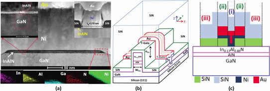
Figure 1: (a) Cross-sectional HR-TEM image of InAlN/GaN HEMT structure, cross-sectional area EDX mapping for different elements in InAlN/GaN nano-channel(NC): inset 1 - InAlN/AlN/GaN heterostructure; inset 2 - T-gate NC Fin-HEMT. (b) Three-dimensional schematic view of Triple T-gate on InAlN/GaN nano-channel. (c) Schematic cross-section of T-shape gate configuration with different stress regions [(i) SiN/Au/Ni stress layers, (ii) SiN/Au/Ni/SiN stress layers and (iii) SiN/SiN stress layers] to InAlN/GaN nano-channel.
One fin-HEMT device with silicon nitride passivation/stress achieved a maximum drain current of 3940mA/mm of effective gate width (200nm), and transconductance of 1417mS/mm at 6V drain bias. The researchers comment: "The observed IDmax and gmmax values are the highest ever reported in the literature for NC Fin-HEMTs on Si(111)."
Conventional passivated InAlN/GaN HEMTs produced along with the fin-HEMTs achieved 1225mA/mm maximum drain current. AlGaN/GaN HEMTs on very expensive silicon carbide (SiC) substrates have achieved 4000mA/mm drain current.
The researchers were variously associated with Singapore's Nanyang Technological University and Institute of Materials Research and Engineering (IMRE), along with Ohio State University in the USA.
The epitaxial structure was grown on high-resistivity (111) silicon by metal-organic chemical vapor deposition (MOCVD). The barrier layer was In0.17Al0.83N, separated from the GaN buffer/channel by an AlN spacer. Measurements on Hall van-der-Pauw structures gave a carrier density of 2.74x10¹³/cm2 and mobility of 760cm2/V-s for the two-dimensional electron gas (2DEG) channel at 300K.
Device fabrication began with mesa isolation and nano-channel fin formation. The fin height was 12nm. The widths were 176nm or 314nm. The nickel/gold 3D triple gate was formed into T-shapes with optional silicon nitride passivation/stress layer.
The performance of the NC fin-HEMTs was compared with conventional HEMTs. The gate lengths of all devices were 170nm. Also, the devices had fixed dimensions for source-gate (850nm) and gate-drain (1800nm) separation.
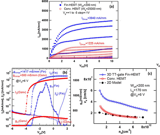
Figure 2: (a) Drain current versus voltage (IDS-VDS), (b) drain current and transconductance (ID(gm),|Ig|-Vg) transfer characteristics of conventional InAlN/GaN HEMTs and 3D TT-gate InAlN/GaN NC Fin-HEMTs. (c) Calculated electron velocity (ve) for 3D TT-gate InAlN/GaN NC fin-HEMT, conventional HEMT, and 2D model.
The researchers estimated an electron velocity of 6.0x107cm/sec, compared with 3.17x107cm/sec for the conventional HEMT. The fin-HEMT value is also greater than reported drift velocities for InAlN/AlN/GaN structures at high electric field of 3.2x107cm/sec, although AlGaN/GaN structures have achieved 6.8x107cm/sec with 0.3MV/cm field at 4.2K. The researchers suggest that the 3D geometry of the fin-HEMT combined with stress could alter the optical-phonon spectrum or scattering rates that control electron velocities in the 2DEG.
Devices without silicon nitride stress/passivation demonstrated poorer performance. Raman spectroscopic analysis showed that the silicon nitride introduced tensile stress to the fin structures.
InAlN GaN fin-HEMT HEMT GaN MOCVD
http://dx.doi.org/10.1063/1.4906970
The author Mike Cooke is a freelance technology journalist who has worked in the semiconductor and advanced technology sectors since 1997.


