


- News
6 February 2015
Spreading current with silver nanowires and carbon nanotubes
Researchers in China have developed a hybrid silver nanowire/carbon nanotube (AgNW/CNT) current-spreading layer for aluminium gallium indium phosphide (AlGaInP) light-emitting diodes (LEDs) [Bai Liu et al, Appl. Phys. Lett., vol106, p033101, 2015].
Based at Beijing University of Technology, Beijing University of Chemical Technology and Tsinghua University, the team used the Ag NWs to redistribute carriers between the CNTs (Figure 1). Without the NWs, the rate of carrier transfer between CNTs is low due to a high intertube contact resistance.
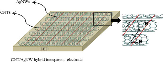
Figure 1: Schematic of LED with CNT/AgNW hybrid film as transparent conducting layer.
The researchers comment: "The hybrid film takes advantage of the extremely high mobility and conductivity of individual CNTs and avoids the high intertube contact resistance of CNT networks by including AgNWs. The carriers are not only transported along the CNTs but also between CNTs through the AgNW bridges in a vertical direction, providing a symmetric carrier distribution."
The AlGaInP LEDs consisted of an 800nm active region with 60-period (Al0.5Ga0.5)0.5In0.5P/(Al0.1Ga0.9)0.5In0.5P multi-quantum well. The active region was sandwiched between n- and p-type cladding layers of (Al0.7Ga0.3)0.5In0.5P. The LED heterostructure was grown on a distributed Bragg reflector (DBR) consisting of 15 layer pairs of Al0.6Ga0.4As/AlAs on a 100nm gallium arsenide (GaAs) buffer. The growth substrate was n-GaAs. The structures also included a final 500nm p-GaP window layer.
The p-electrode consisted of a 100μm-diameter region of gold/beryllium-gold/gold. The n-electrode was gold-germanium-nickel/gold sputtered onto the back-side of the growth substrate. The CNTs were drawn continuously from multi-walled CNT arrays, adhering through Van der Waals forces. The process resulted in 'a super-aligned CNT (SACNT) film', according to the researchers. Titanium/gold was deposited and patterned on the p-electrode to make sure the SACNT film remained in place. The resulting LED chips were 300μmx300μm.
Optical transmission of 550nm wavelength through the SACNT was about 85%. To increase the light transmission the researchers used a 30-second oxygen plasma etch to decrease the density of tubes, increasing transmission to 96%. After the etch, the Ag NWs were spin-coated onto the CNTs. The structure was then annealed at 200°C for 10 minutes to improve the electrical contact between the Ag NWs and CNTs.
By varying the Ag NW concentration in the spin-coating process, the light transmission (T550nm) could be traded off against sheet resistance (Rs). "For AgNW concentrations of 0.25mg/ml and 0.5mg/ml, T550nm (Rs) of the hybrid films was 93% (88Ω/square) and 90% (23Ω/square), respectively," the researchers report. The sharp drop in resistance is attributed to a typical percolation threshold effect, where a small increase in connectivity of a random network creates conduction paths across a space.
One effect of the AgNW/CNT hybrid film was to slightly reduce the LED forward voltage at 20mA from 2.1V to 2.0V (Figure 2). This indicates a reduced series resistance loss.
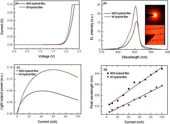
Figure 2: (a) Current versus voltage, and (b) electroluminescence (EL) spectra at 20mA (inset EL images at 2.5mA of 2.5μmx2.5μm area around electrodes of control and hybrid-film LED wafers), and dependence of (c) light output, and (d) peak wavelength on injection current of AlGaInP LEDs with and without AgNW/CNT hybrid film.
The electroluminescence (EL) was "greatly enhanced" at 20mA by the presence of the hybrid AgNW/CNT current-spreading layer, despite an estimated 10% optical loss. The researchers add, "The high surface roughness of the hybrid film further increased the light output of the LED." This was presumably due to better transmission of light – rather than reflection – from the device-air interface.
The emission pattern of the LED chip without hybrid film showed current crowding around the p-electrode. By contrast, the emission from the LED with hybrid film was bright and uniform across the chip. The integrated intensity of the hybrid-film LED was 1.6x that of the control device at 20mA. The 1.6 enhancement factor continued up to 60mA injection. Beyond that, the enhancement was limited by self-heating effects. The researchers say the current-spreading effect was reduced by the higher temperature in the film.
With increased current injection, the emission peaks of both devices red-shifted – at the rates 0.1nm/mA and 0.15nm/mA for the hybrid-film and control devices, respectively. At 100mA, the corresponding total red-shifts were 9.7nm and 13.11nm.
LEDs AlGaInP Hybrid silver nanowire carbon nanotube
http://dx.doi.org/10.1063/1.4906351
The author Mike Cooke is a freelance technology journalist who has worked in the semiconductor and advanced technology sectors since 1997.


