


- News
28 January 2015
Discrepancy in carrier density estimates for HVPE GaN templates
Researchers at Raja Ramanna Centre for Advanced Technology in India have studied different techniques for measuring the electron transport properties of gallium nitride on sapphire grown by hydride vapor phase epitaxy (HVPE) and metal-organic vapor phase epitaxy (MOVPE) [Abhishek Chatterjee et al, Appl. Phys. Lett., vol106, p023509, 2015]. MOVPE templates give relatively similar estimates for carrier density in Hall and capacitance-voltage (CV) analyses. However, CV carrier density measurements on HVPE templates are two orders of magnitude lower than for Hall estimates.
Pre-grown commercial GaN templates on sapphire are commonly used to avoid tricky and time-consuming growth of thick buffer layers of the order of microns. Instead, using commercial templates, manufacturers and researchers can focus on growing the critical heterostructure layers for optoelectronic and high-frequency/power electronic applications. HPVE has a higher growth rate than MOVPE, leading to a cost advantage.
The Raja Ramanna researchers studied commercial templates produced using HVPE and MOVPE. The researchers found that Hall and CV measurements on HVPE templates on sapphire gave radically different estimates for carrier density (Figure 1).
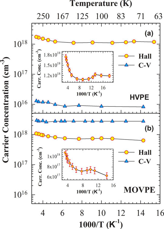
Figure 1: Carrier concentration versus temperature recorded by Hall and C-V techniques for (a) HVPE- and (b) MOVPE-grown GaN templates. Insets: Hall concentration values plotted on linear scale with inverse temperature.
The researchers comment that, for the HVPE templates, "such a large difference in carrier concentration values is associated with the formation of a degenerate layer at the layer-substrate interface, which consists of a large density of threading screw and edge dislocations. Clustering of impurities around these dislocations leads to the formation of a highly conducting parallel channel for the carriers which severely affects the transport characteristics of HVPE-grown GaN templates."
The conducting channel at the sapphire/GaN layer interface could adversely affect the performance of devices using such templates. Making the GaN layer thicker reduces the parasitic effect of the interface channel, dependent on doping and dislocation density.
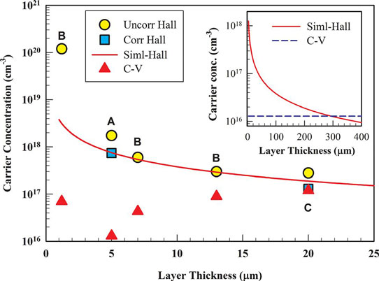
Figure 2: Carrier concentration values obtained from conventional Hall (Uncorr-Hall), two-layer model (corr-Hall), and C-V measurements as functions of layer thickness for HVPE GaN template. Extrapolated carrier concentration curve is from two-layer model (Siml-Hall). Inset: comparison of numerically calculated Hall values with carrier concentration measured by C-V technique HVPE GaN templates.
The researchers compared results with different thicknesses of HVPE GaN from their own and previous research (Figure 2), along with a corrected Hall value based on a two-conducting-layer model of Look and Molnar, reported in 1997 [http://dx.doi.org/10.1063/1.119176]. While the Hall measurements of the other groups line up with the two-layer Hall simulation, the CV values are still discrepant, except for Look and Molnar's result with a 20μm layer (C), due to higher doping. The Raja Ramanna researchers believe that their CV results would line up with the corrected Hall result at around 300μm layer thickness. The researchers' samples were 5μm thick (A). The (B) points were from http://journals.cambridge.org/action/.
HVPE MOVPE GaN templates GaN Sapphire
http://dx.doi.org/10.1063/1.4906286
The author Mike Cooke is a freelance technology journalist who has worked in the semiconductor and advanced technology sectors since 1997.


