


- News
21 January 2015
First group-IV lasers grown on silicon by FZ Jülich and the Paul Scherrer Institute
In cooperation with international partners, Germany’s Forschungszentrum Jülich and the Paul Scherrer Institute (PSI) in Villigen, Switzerland have presented what is claimed to be the first semiconductor laser consisting solely of main group IV elements (‘Lasing in direct bandgap GeSn alloy grown on Si’, Wirths et al, Nature Photonics; DOI: 10.1038/nphoton.2014.321). The germanium-tin (GeSn) laser can be applied directly onto silicon, hence facilitating optical data transmission on computer chips (faster than possible via copper wires and requiring only a fraction of the energy).
“Signal transmission via copper wires limits the development of larger and faster computers due to the thermal load and the limited bandwidth of copper wires,” says professor Detlev Grützmacher, director at Jülich’s Peter Grünberg Institute, Semiconductor Nanoelectronics (PGI-9). “The clock signal alone synchronizing the circuits uses up to 30% of the energy – energy which can be saved through optical transmission,” he adds. “The integration of optical components is already well advanced in many areas,” continues Grützmacher PGI’s head of Semiconductor Nanoelectronics (PGI-9). “However, in spite of intensive research, a laser source that is compatible with the manufacturing of chips is not yet achievable.”
Suitable material for chip production
Compared with group IV silicon, typical telecom lasers made of group III-V elements, such as gallium arsenide (GaAs) for example, are costly and, due to their different crystal properties, cannot be grown directly on silicon (needing instead to be produced separately and then bonded to a silicon wafer). Also, device lifetime is greatly reduced due to the thermal expansion coefficients of these elements being significantly different from that of silicon.
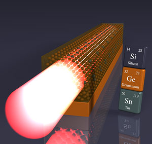 Picture: Schematic of the germanium-tin (GeSn) laser, applied directly onto the silicon wafer (blue) using an intermediate layer of pure germanium (orange). Copyright: Forschungszentrum Jülich
In contrast, group IV semiconductors such as silicon and germanium can be integrated into the manufacturing process without any major difficulties. However, neither element is very efficient as a light source, due to having an indirect energy bandgap. In contrast to direct-bandgap semiconductors, they emit mostly heat and just a small amount of light when excited. Many research groups are hence trying to manipulate the material properties of germanium so that it can amplify optical signals, making it a usable laser source.
Compound with a high tin content
Jülich’s Peter Grünberg Institute says that it has now created the first ‘real’ direct-bandgap group IV semiconductor laser by combining germanium and tin (which is also a group IV element). “The high tin content is decisive for the optical properties,” comments PhD student Stephan Wirths. “For the first time, we were able to introduce more than 10% tin into the crystal lattice without it losing its optical quality,” he adds. “The functioning of the laser is so far limited to low temperatures of up to minus 183 degrees Celsius, however,” notes co-author Dr Dan Buca. “This is mainly due to the fact that we worked with a test system that was not further optimized.”
In cooperation with colleagues in professor Siegfried Mantl’s group at PGI-9, Wirths applied the laser directly onto a silicon wafer whose properties were subsequently measured at the Paul Scherrer Institute, where PhD student Richard Geiger fabricated the laser structures. “That way, we were able to demonstrate that the germanium-tin compound can amplify optical signals, as well as generate laser light,” says Dr Hans Sigg of PSI’s Laboratory for Micro and Nanotechnology.
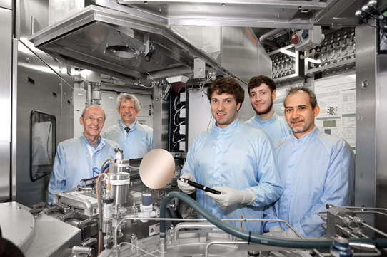
Picture: (From left) Professor Siegrfried Mantl, professor Detlev Grützmacher, Stephan Wirths, Nils von den Driesch, and Dr Dan Mihai Buca of the Peter Grünberg Institute (PGI-9), standing next to a CVD system used to prepare and develop parts of the new laser. Copyright: Forschungszentrum Jülich
For the demonstration, the laser was excited optically. Currently, Buca’s group at Jülich is working on linking optics and electronics even more closely. The next big step will be generating laser light with electricity instead, and without the need for cooling if possible. The aim is to create an electrically pumped laser that functions at room temperature.
New wavelength for new applications
GeSn absorbs and emits light in a wavelength range of about 3µm. Many carbon compounds, such as in greenhouse gases or biomolecules, also display strong absorption lines at this boundary between near- and mid-wavelength infrared. Hence, sensors made of GeSn promise a new possibility for detecting these compounds.
Along with computer chips, completely new applications that have not been pursued so far for financial reasons may thus benefit from the new laser material. Examples include gas sensors or implantable chips for medical applications that can gather information about blood sugar levels or other parameters via spectroscopic analysis. In the future, cost-effective, portable sensor technology – which may be integrated into a smart phone – could supply real-time data on the distribution of substances in the air or ground, contributing to better understanding of weather and climate development.
The research was funded partly by the Swiss National Science Foundation (SNF). Funding for CVD growth came from the European Community’s Seventh Framework Program (grant no. 619509; project E2SWITCH) and the BMBF project UltraLowPow (16ES0060 K).


