


- News
21 January 2015
Prospect of accurate p-type silicon-doped gallium arsenide antimonide
Researchers at Japan's NTT Device Technology Laboratories have used silicon (Si) doping to achieve p-type conduction in gallium arsenide antimony (GaAsSb) produced with metal-organic chemical vapor deposition (MOCVD) on indium phosphide (InP) [Haruki Yokoyama and Takuya Hoshi, Jpn. J. Appl. Phys., vol54, p015506, 2015]. Yokoyama and Hoshi write: "This is the first time that p-type doping into GaAsSb layers has been achieved by MOCVD using Si as a dopant."
These researchers believe that the resulting p-GaAsSb could be useful for heterojunctions with InP and InGaAs with improved device performance in heterojunction bipolar transistors (HBTs), tunnel diodes and tunnel field-effect transistors.
Alternative p-dopants for GaAsSb suffer from high levels of diffusion, which makes accurate doping profiles difficult to achieve. Carbon (C) is also a p-dopant for GaAsSb with a relatively low diffusion rate, but the precursor used to supply C atoms, tetrabromomethane (CBr4), has an etching effect on GaAsSb, again compromising doping profiles.
Silicon also has a low diffusion coefficient, but previous work producing Si-doped GaAsSb by MOCVD has resulted in n-type conduction. Although Si is an n-type impurity in GaAs, it is a p-type impurity in GaSb.
Yokoyama and Hoshi hoped that different growth conditions might lead to p-type conduction from Si-doped GaAsSb. Previous work reported by others in 1988 with molecular beam epitaxy (MBE) supported this: GaAsSb showed a shift from n-type to p-type conductivity as the growth temperature increased. MOCVD processes tend to be preferred by manufacturers.
Yokoyama and Hoshi used MOCVD carried out in a close-coupled showerhead reactor on (001) semi-insulating iron-doped InP wafers. The source materials were triethylgallium (TEGa), arsine (AsH3) and trimethylantimony (TMSb) in hydrogen carrier gas. The silicon doping was achieved with disilane (Si2H6). The growth pressure was 125mbar.
Undoped lattice-matched GaAsSb/InP samples were found to have p-type conductivity. However, silicon doping shifted this to n-type when MOCVD was carried out at 530°C (Figure 1). At 580°, silicon doping instead increased the hole density, giving stronger p-type behavior.
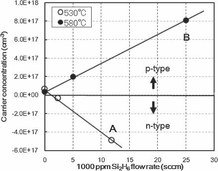
Figure 1: Si2H6 flow rate dependence of carrier concentration in Si-doped GaAsSb layers.
Yokoyama and Hoshi comment: “These results confirm that there is a proportional relationship between the Si2H6 flow rate and carrier concentration, regardless of conductivity type. This indicates that precise control of p- and n-type carrier concentration in Si-doped GaAsSb layer is possible.”
The mobility behavior of the samples was similar to that achieved for GaAsSb samples produced using MBE (Figure 2). Comparison was made with silicon-doped MBE GaAsSb for the n-type low-temperature MOCVD material and with carbon-doped MBE GaAsSb for the p-type layer.
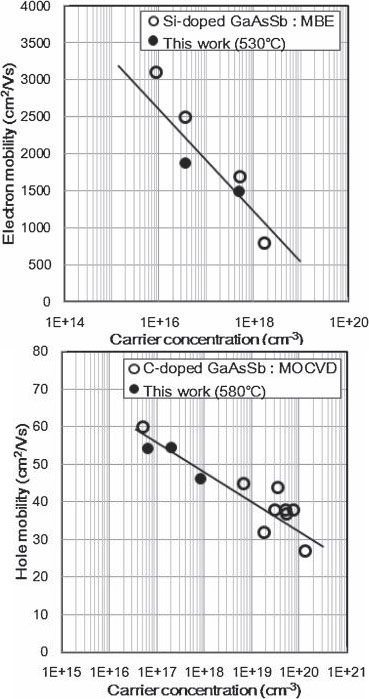
Figure 2: (a) Relationship between electron mobility and electron carrier concentration in Si-doped GaAsSb layers grown at 530°C, compared with MBE GaAsSb:Si. (b) Relationship between hole mobility and hole carrier concentration in Si-doped GaAsSb layers grown at 580°C, compared with MBE GaAsSb:C.
Secondary-ion mass spectrometry (SIMS) showed that the silicon doping concentration was constant through the deposited layers. The activation ratio of electron carrier concentration to silicon concentration was 0.33 for a 530°C GaAsSb layer with 1.5x10¹⁸/cm3 doping density. The hole/silicon ratio was 0.27 for 580°C GaAsSb with 3x10¹⁸/cm3 silicon density.
Si-doped MBE GaAsSb has been reported with 0.392 activation of 1.27x10¹⁸/cm3 doping. C-doped MBE GaAsSb activation has been measured close to 1. The low activation of Si-GaAsSb does not impact the mobility performance (Figure 2b). “Since alloy scattering becomes dominant in GaAsSb, it may eliminate the effect of inactivation,” write Yokoyama and Hoshi.
http://dx.doi.org/10.7567/JJAP.54.015506
The author Mike Cooke is a freelance technology journalist who has worked in the semiconductor and advanced technology sectors since 1997.


